Low offset rail-to-rail operational amplifier

a technology of operating amplifier and rail-to-rail, which is applied in the direction of amplifiers, amplifier modifications to reduce detrimental impedence, and amplifiers with semiconductor devices/discharge tubes, etc. it can solve the problems of bipolar transistors with finite input impedance and add significant cost, and create inaccuracies in the tens or hundreds of percent when dealing with low-level signals, and achieves simple and auto-routing rail-to-rail. low

Inactive Publication Date: 2006-05-11
SHULER ROBERT LUCKETT JR +1
View PDF5 Cites 24 Cited by
  • Summary
  • Abstract
  • Description
  • Claims
  • Application Information

AI Technical Summary

Benefits of technology

[0020] A further object of the invention is to provide a simplified and auto-routable rail-to-rail operational amplifier with low offset.

Problems solved by technology

In a properly designed circuit, the small residual offset results from unavoidable imperfections in the devices from which the amplifier input stage is made.
Bipolar junction transistor technology allows construction of amplifiers with low offset, but bipolar transistors have finite input impedance and add significant cost as compared with complementary metallic oxide semiconductor (CMOS) technology, which is very economical in bulk and provides near infinite input impedance.
This creates inaccuracies in the tens or hundreds of percent when dealing with low-level signals.
Also, many circuits have the unfortunate effect of multiplying the input offset by gain or some other large factor.
If more than two gain stages are present, ordinary Miller compensation may not be sufficient.
Mismatch can result from small differences in the actual geometry of supposedly identical devices, or from differences in the electrical properties of the region in which the device is fabricated.
However, making the channel too long results in a slow amplifier that is difficult to stability compensate, and results in the output transistors being unreasonably large due to scaled matching.
Dynamic (switched) offset reduction methods can be made to work very well, however they add a great deal of complexity and thus area.
Rail-to-rail op amps of the higher voltage variety may violate the voltage limitations of a particular technology.
Amps of the complementary input pair variety have the unfortunate effect that their input offset voltage varies over the common mode range, since the two input pairs will have different offset characteristics.
The combining circuitry, which is invariably asymmetric, may further disturb offset characteristics.
This means the amp must be made faster by using smaller and higher aspect ratio devices (ratio of channel width to length for FET's), which in turn increases the variability of offset with common mode voltage, and further pushes up the switching rate in a vicious cycle.

Method used


Image

  • Low offset rail-to-rail operational amplifier
  • Low offset rail-to-rail operational amplifier
  • Low offset rail-to-rail operational amplifier

Examples


embodiment

Preferred Embodiment

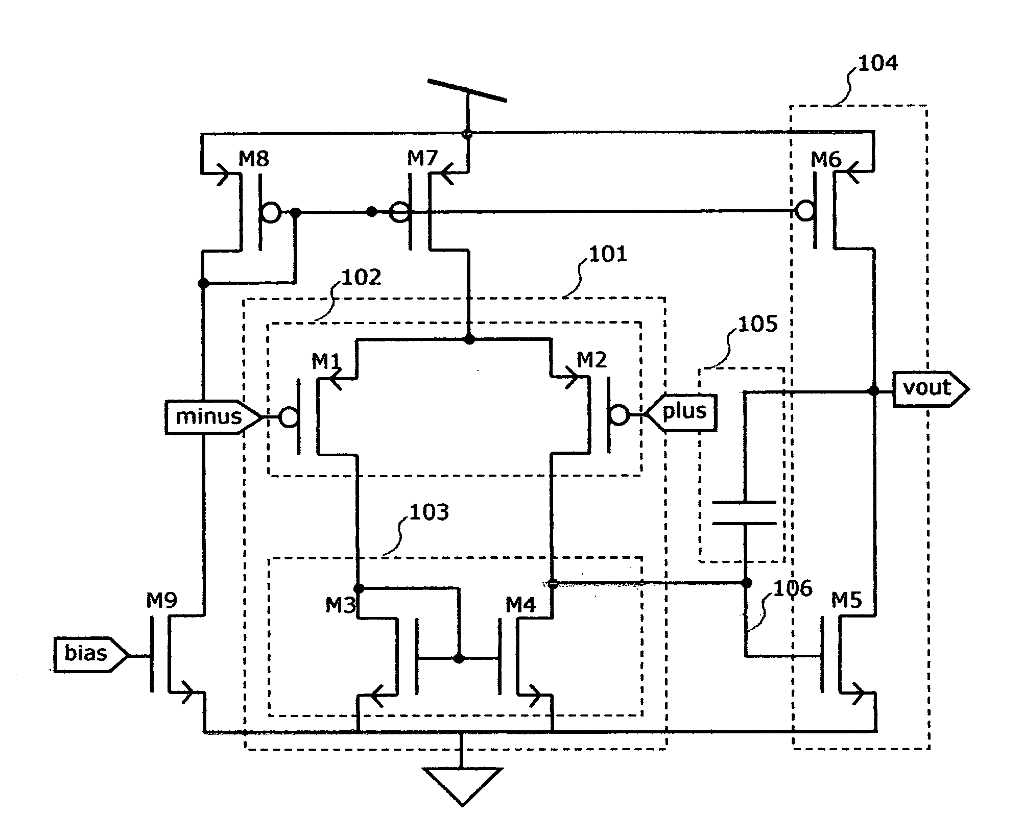
[0050] Turning to FIG. 4 there is shown the preferred embodiment of the present invention. A differential input voltage level shift circuit is provided in two parts 401 to shift the plus input and 402 to shift the minus input. The inputs plus and minus are connected to a first input stage differential pair 405 and to the level shift circuit. The shifted input voltages appearing at the outputs of the level shift circuit on nodes 403 and 404 are connected to a second input stage differential pair 406 which is of the same type P or N as the first input differential pair, and will usually be identical. The differential outputs from the two input differential pairs are recombined by simple current summation at nodes 407 and 408, which are also connected to the single input stage current mirror 409.

[0051] While FIG. 4 shows P-type differential pairs, the skilled practitioner easily recognizes the same design principles apply to an amplifier made with N-type pairs, or ...


PUM


Abstract

An operational amplifier with a first stage differential input circuit having low aspect ratio devices of size chosen to achieve a low offset voltage, and an output stage having high aspect ratio devices able to operate at higher frequencies than the input stage, provides an amplifier with low static offset and requiring only a small compensation circuit due to the wide separation of frequency response poles. Adding a third stage gives a high gain design that can be stabilized with nested miller compensation. Adding a second differential input circuit of the same type as the first, and a level shifter, provides rail-to-rail operation without disturbing the low offset properties.

Description

BACKGROUND OF THE INVENTION [0001] This invention relates generally to the field of integrated electronic circuits and more specifically to low offset rail-to-rail operational amplifiers. [0002] Operational amplifiers having a differential input and a large gain are an essential building block of many electronics circuits. The offset of the amplifier is that voltage difference between the positive and negative input terminals which is interpreted as zero difference by the amplifier. In a properly designed circuit, the small residual offset results from unavoidable imperfections in the devices from which the amplifier input stage is made. The input common mode range (CMR) of the amplifier refers to the range of the average of the two input voltages over which the amplifier will operate. Basic amplifier designs will usually stop working if both input voltages approach one or the other of the input supply voltages (rails). [0003] Bipolar junction transistor technology allows constructi...

Claims


Application Information

Patent Timeline
Patent Type & Authority Applications(United States)
IPC IPC(8): H03F1/14
CPCH03F1/08H03F1/14H03F3/3022H03F3/45183H03F3/45744H03F2203/45512H03F2203/45652
Inventor SHULER, ROBERT LUCKETT JR.ASKEW, R. SCOTT
Owner SHULER ROBERT LUCKETT JR
Why Eureka
Try Eureka