Source synchronous transfer scheme for a high speed memory interface

a memory interface and synchronous transfer technology, applied in logic circuit coupling/interface arrangement, generating/distributing signals, instruments, etc., can solve the problems of reducing the band pass of a system, affecting the band pass of the entire computer system, and limiting data transfer rates

Inactive Publication Date: 2001-03-06
CHARLES A JOHNSON
View PDF21 Cites 28 Cited by
  • Summary
  • Abstract
  • Description
  • Claims
  • Application Information

AI Technical Summary

Problems solved by technology

Although these benefits can be substantial, shared resources may reduce the band pass of a system if not carefully used and designed.
If a processor is in the critical path of a computer system and it is not allowed to access the shared resource, the band pass of the entire computer system may suffer.
Accordingly, data transfer rates are typically limited by the maximum clock rate of the system.
Several potential problems are encountered when increasing the maximum clock rate of the system.
Thus, timing constraints on the data transmittal path become more acute as the transfer clock rates are increased.

Method used


Image

  • Source synchronous transfer scheme for a high speed memory interface
  • Source synchronous transfer scheme for a high speed memory interface
  • Source synchronous transfer scheme for a high speed memory interface

Examples


Embodiment Construction

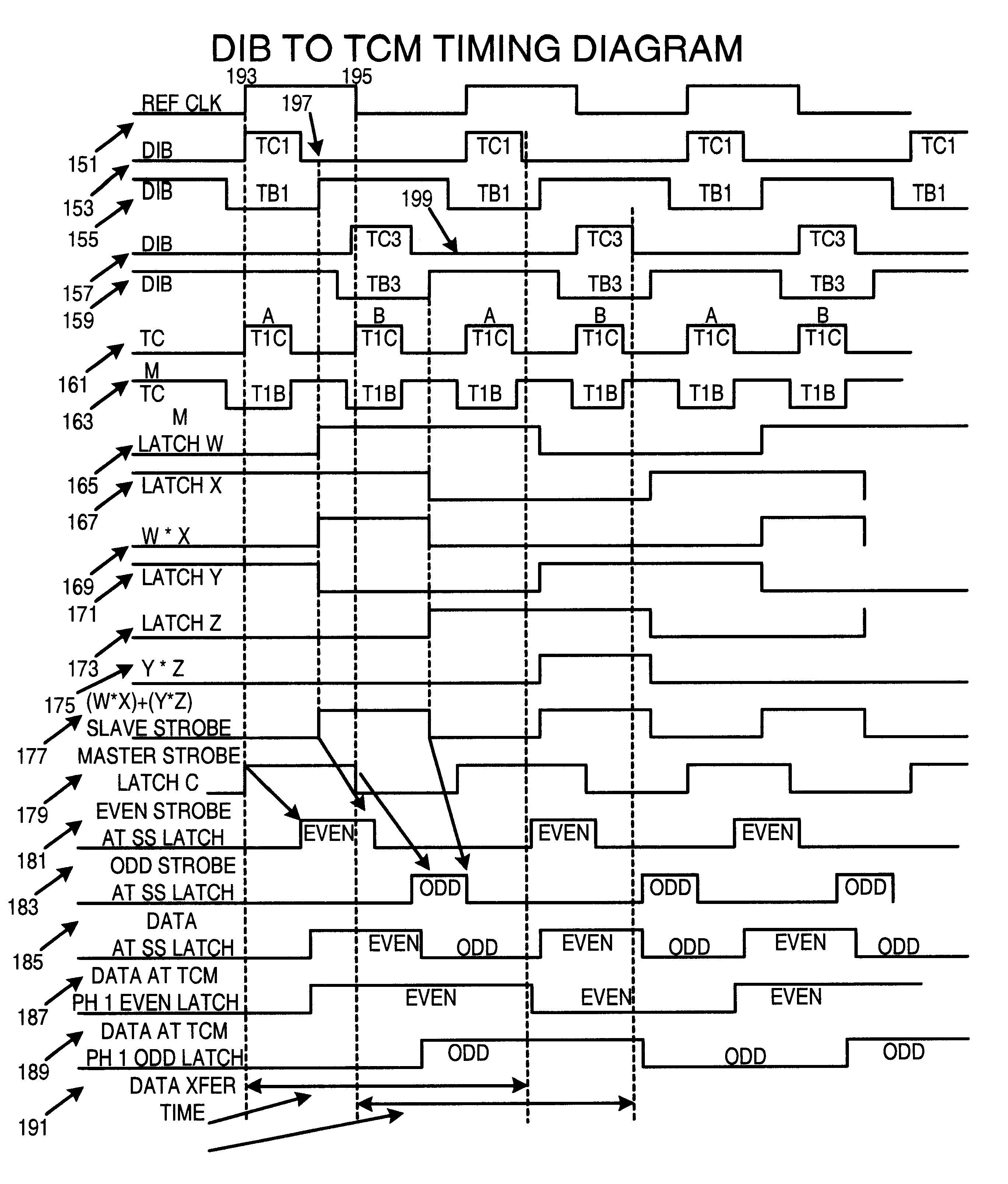
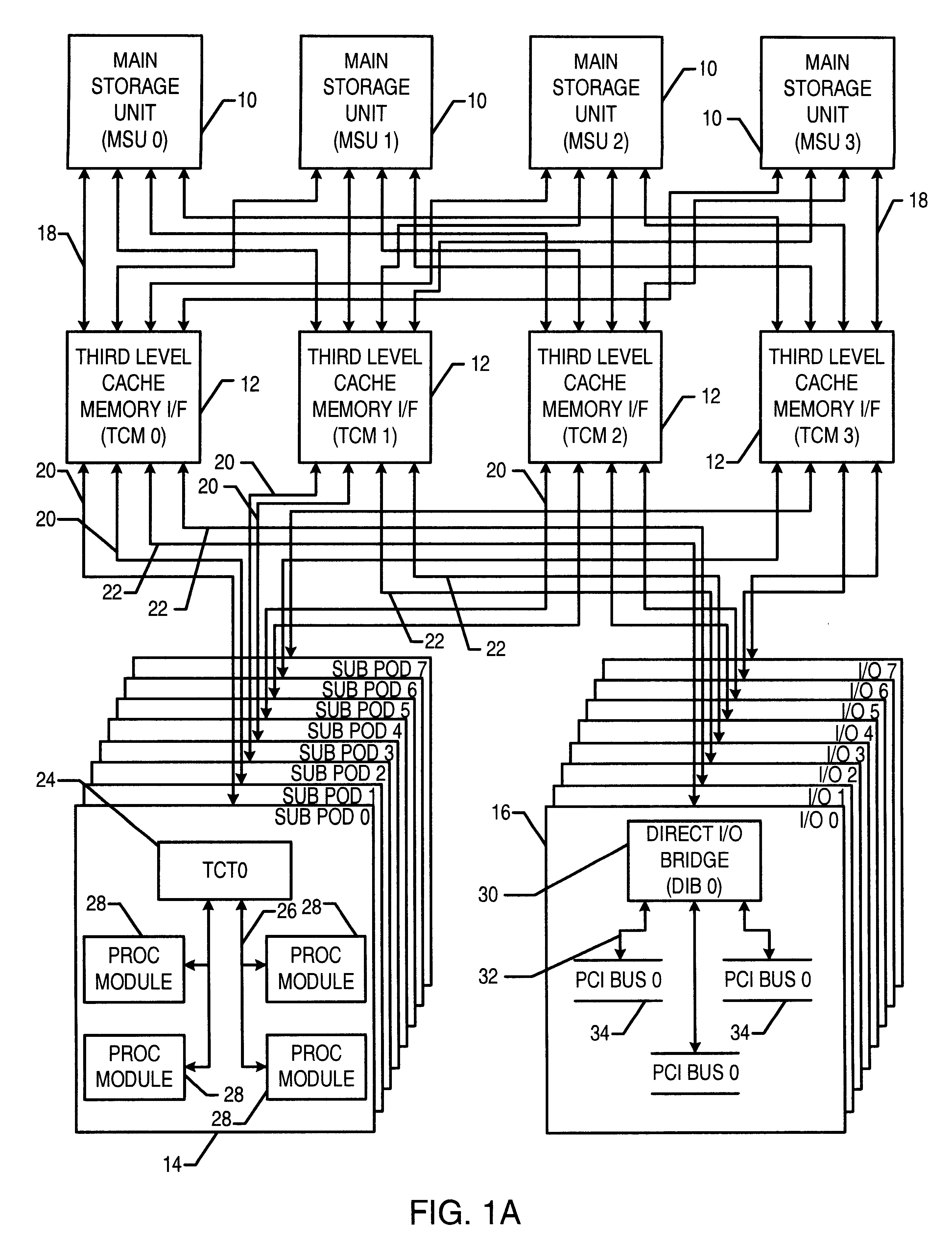
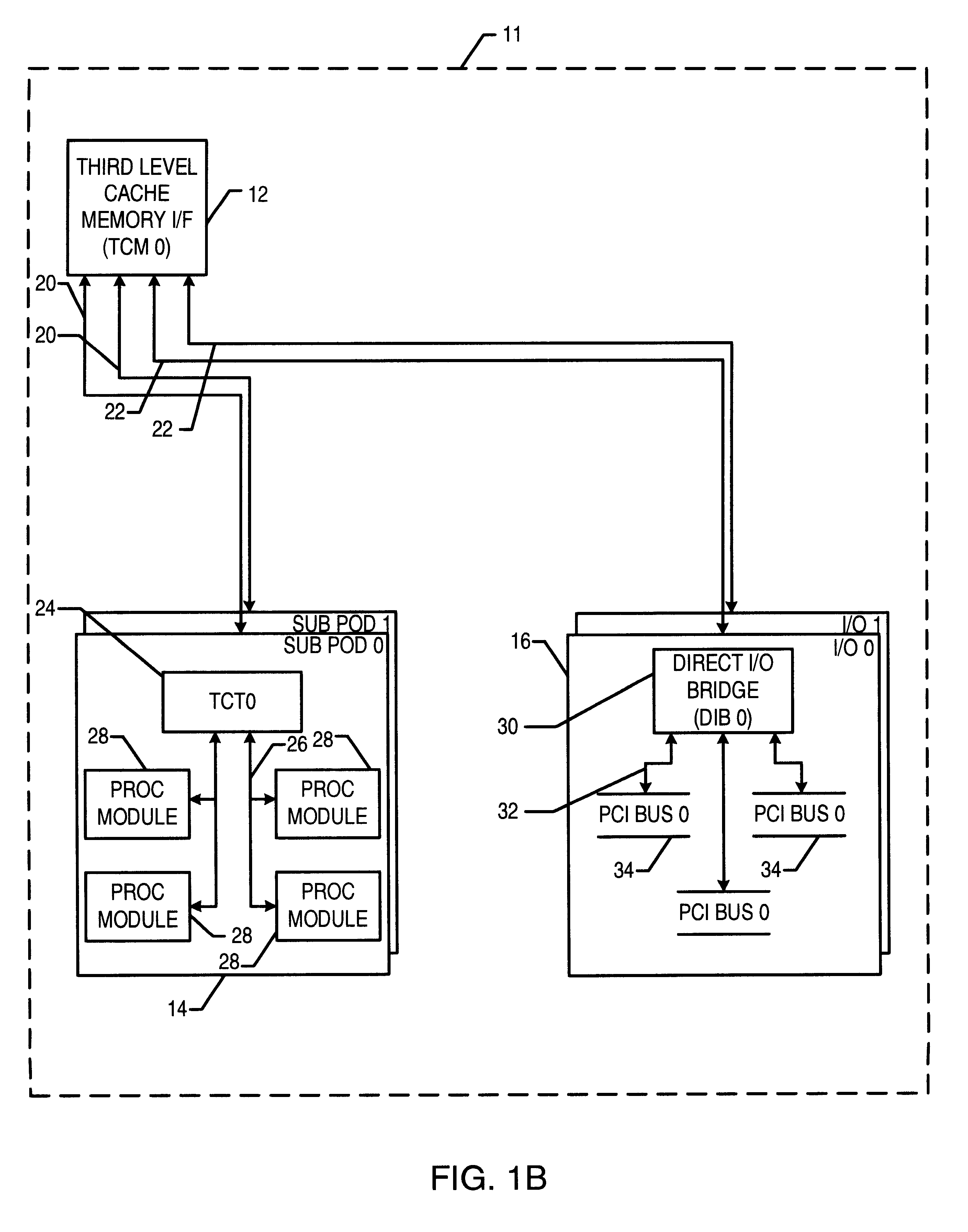
=L (element 235) and DIB MODE=H (element 237)) for either the DIB interface at a 100 Mhz data rate or for the Cluster interface at a 200 Mhz data rate. FIG. 7 shows the TCM conditioned for the DIB interface. In general, the TCM 221 which cycles at twice the rate of the DIB 223 transmits data 202 on the bus 219 ever TCM TC2 (FIG. 8, element 259). The even data is transmitted on the TCM TC2_A and the odd data is transmitted on the TCM TC2_B. The data 200 is the same as data 202 and is re-clocked into the source phase latch (FIG. 5, element 105) with TCM TC4 (FIG. 8, 263) in order to match the clock rate of the DIB which is half that of the TCM.

In FIG. 7, data groups 200 and 202 (same data) are passed on to the input of source phase latch 205. When source phase latch 205 is clocked, the multiplexed even / odd data group signal 219 is concurrently transmitted to the receiving DIB ASIC 223 on the data bus along with two strobe signals (master 204 and slave 206), which have low skew with re...


PUM


Abstract

Data transfer scheme wherein data transfer rates can be effectively doubled with no increase in the clock speed of the interface. This is accomplished by allowing more than one data transfer to occur on a single clock cycle. This transfer scheme increases the transfer rate of the interface by multiplexing two data groups on the same interface. These data groups are transmitted from a source phase latch at approximately the same time as two strobe signals which have low skew with respect to the data. The master and slave strobe signals are logically combined to create an even latch enable signal and an odd latch enable signal that are used to latch and de-multiplex the multiplexed data groups at a receiving end of a pair of flow-though source synchronous latches.

Description

1. Field of the InventionThe present invention relates to storage interfaces in symmetrical multiprocessor systems, and more specifically, to a source synchronous transfer scheme that may increase the data rate over normal synchronous transfer methods.2. Description of the Prior ArtIn most general purpose, stored program, digital computers, it is desirable to have shared resources contained therein. Each of the shared resources may be designed to service a number of users. Possible shared resources may include a bus, a memory, a processor, or any other element within the computer system. The concept of utilizing shared resources has been used for several years to decrease the number of components within a computer system thereby increasing the cost effectiveness of the system. The use of shared resources also reduces the overall size and power requirements of the computer system.Although these benefits can be substantial, shared resources may reduce the band pass of a system if not ...

Claims


Application Information

Patent Timeline
Patent Type & Authority Patents(United States)
IPC IPC(8): G06F13/42
CPCG06F13/4243
Inventor MAAHS, DAVID A.MALEK, ROBERT M.BAUMAN, MITCHELL A.
Owner CHARLES A JOHNSON
Why Eureka
Try Eureka