Large grained polycrystalline silicon and method of making same

a polycrystalline silicon and large-grain technology, applied in the field of large-grain polycrystalline silicon, can solve the problems of substantial material loss, higher price per watt of electricity generated by these modules,

Inactive Publication Date: 2006-05-25
CALIFORNIA INST OF TECH
View PDF2 Cites 70 Cited by
  • Summary
  • Abstract
  • Description
  • Claims
  • Application Information

AI Technical Summary

Problems solved by technology

However, the price per watt of the electricity generated by these modules is higher than desired due to the high energy costs of refining silicon into ingots for use in traditional solar cells.
Moreover, a substantial amount of material is lost once the ingots are sawed into wafers.

Method used


Image

  • Large grained polycrystalline silicon and method of making same
  • Large grained polycrystalline silicon and method of making same
  • Large grained polycrystalline silicon and method of making same

Examples


first embodiment

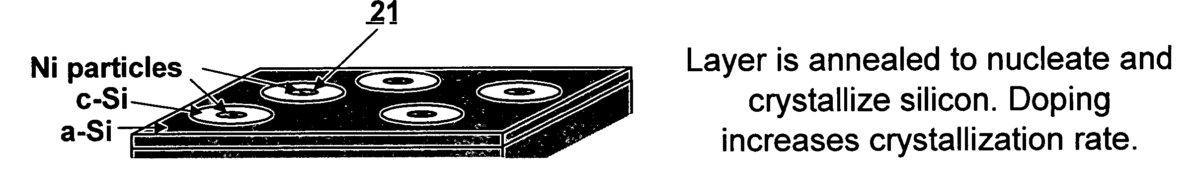
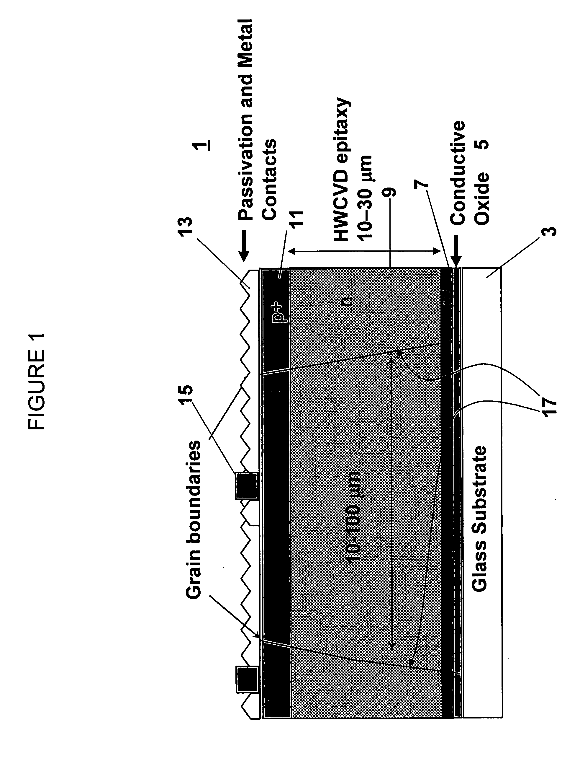
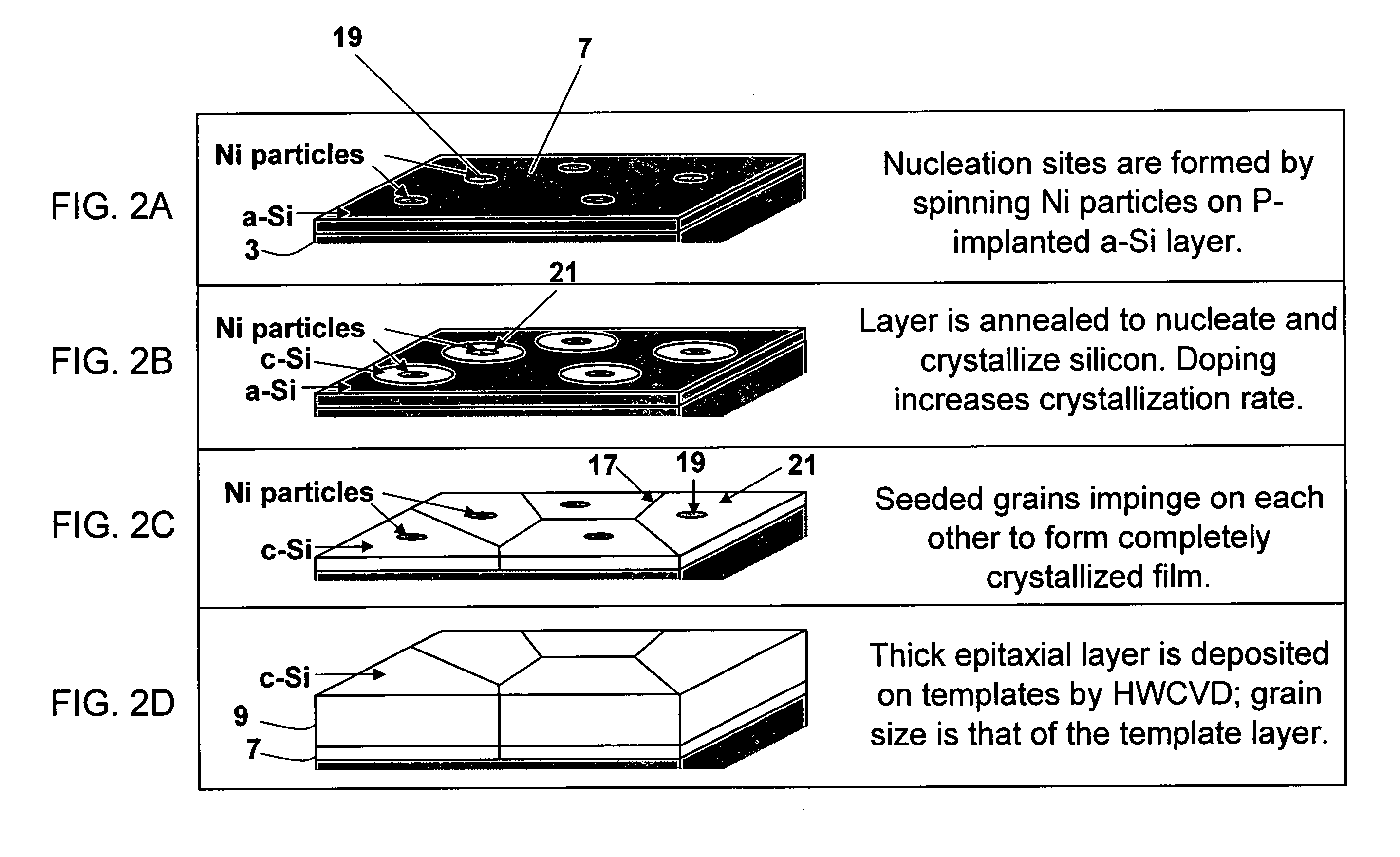
[0013] The first embodiment provides a silicon structure comprising (a) a polysilicon template layer and (b) an epitaxial polysilicon layer formed on the template. The template is preferably a so-called selective nucleation single phase epitaxial (SNSPE) template comprising crystallization catalyst residue. In other words, the template comprises a polysilicon layer which is formed by the so-called selective nucleation and solid phase epitaxy (SNSPE), which is also known as metal induced crystallization (MIC) or catalyst mediated crystallization method. In the SNSPE or MIC process, an amorphous silicon (a-Si) or a relatively small grain polysilicon layer is formed on a substrate. This layer is then contacted with a crystallization promoting catalyst material. This may be done by forming the catalyst on the layer, by forming the layer on the catalyst or by introducing the catalyst into the layer. For example, the catalyst may comprise catalyst particles which are formed over or under ...

second embodiment

[0033] A second embodiment of invention comprises a method of making polycrystalline silicon structure, comprising annealing in a silicon containing atmosphere an amorphous silicon or polycrystalline silicon layer contacting or containing a crystallization catalyst. The anneal crystallizes the layer (i.e., crystallizes the amorphous silicon or recrystallizes a small grain size polysilicon) to form a polysilicon layer with a large grain size, such as an average grain size of 10-100 microns. This recrystallized layer may then be used as the template layer 7 for epitaxial CVD layer 9 formation of the first embodiment.

[0034] Any suitable silicon containing atmosphere may be used during the crystallization anneal. Preferably, the silicon containing atmosphere comprises a silane atmosphere. However, other silicon bearing gases may be used instead of or in addition to silane. For example, silicon and chlorine bearing gases may be used, such as silicon tetrachloride (SiCl4), thrichrosilane...


PUM

PropertyMeasurementUnit
thicknessaaaaaaaaaa
grain sizeaaaaaaaaaa
softening temperatureaaaaaaaaaa

Abstract

A silicon structure includes a selective nucleating single phase epitaxial (SNSPE) template polysilicon layer containing crystallization catalyst residue, and a hot wire chemical vapor deposited (HWCVD) epitaxial polysilicon layer epitaxially grown on said template layer. The silicon structure may satisfy at least one of the following: 1) a thickness of the SNSPE template layer is less that about 60 nm; 2) a thickness of the HPCVD layer is greater than about 60 nm. The silicon structure may be used in a polysilicon solar cell or other solid state devices. A method of making a polysilicon layer includes providing a first layer comprising an amorphous silicon or a polysilicon layer containing a crystallization catalyst or in contact with a crystallization catalyst, and annealing the first layer in a silicon containing atmosphere to at least partially crystallize the first layer.

Description

CROSS-REFERENCE TO RELATED PATENT APPLICATIONS [0001] This application claims priority to U.S. provisional application No. 60 / 629,676 “Fabrication process for Large-Grained Polycrystalline Thin Film Solar Cells” to Richardson et. al. filed Nov. 19, 2004, which is incorporated herein by reference in its entirety.STATEMENT REGARDING FEDERALLY SPONSORED RESEARCH OR DEVELOPMENT [0002] This invention was made with government support under grant number DE-AC36-99G010337 from the NREL. The United States government may have rights in this invention.FIELD OF THE INVENTION [0003] The present invention is generally directed to large-grain polycrystalline silicon, methods of fabricating large-grain polycrystalline silicon and electronic devices comprising large-grain polycrystalline silicon, such as thin film solar cells. BACKGROUND OF THE INVENTION [0004] The worldwide demand for photovoltaic power modules has grown over the last several years. However, the price per watt of the electricity ge...

Claims


Application Information

Patent Timeline
Patent Type & Authority Applications(United States)
IPC IPC(8): H01L23/48
CPCH01L31/1804H01L31/1872Y02E10/547H01L2924/0002H01L2924/00Y02P70/50
Inventor RICHARDSON, CHRISTINE ESBERATWATER, HARRY A.
Owner CALIFORNIA INST OF TECH
Why Eureka
Try Eureka