Electrostatic discharge testing method and semiconductor device fabrication method

a technology of electrostatic discharge and semiconductor devices, which is applied in the direction of error detection/correction, emergency protective arrangements for limiting excess voltage/current, instruments, etc., can solve the problems of esd breakdown risk, based, erroneously determined, etc., and achieves low accuracy , high accuracy, low accuracy

Inactive Publication Date: 2006-05-25
KK TOSHIBA
View PDF8 Cites 5 Cited by
  • Summary
  • Abstract
  • Description
  • Claims
  • Application Information

AI Technical Summary

Benefits of technology

[0011] Another aspect of the present invention inheres in a method for determining a layout which passes testing for electrostatic discharge in a semiconductor device, including: extracting an electrostatic discharge protection network including pads, nets and protective elements from the layout of the semiconductor device; setting start pads and end pads from the pads in the electrostatic discharge protection network; finding inter-pad voltages with low accuracy between the start pads and the end pads and electrostatic discharge current paths along which the nets and the protective elements are arranged in order

Problems solved by technology

Generally, the risk of an ESD breakdown is high when the inter-pad voltage is high, and it is low when the inter-pad voltage is low.
Moreover, there has also been a case where the magnitude of the ESD withstand voltage, based on only the inter-pad voltage as calculated by the above-described method, was erroneously determined.
The parasitic resistance of interconnects connecting between protective elements greatly affects the ESD withstand voltage.
However, according to this testing method, since ESD testing is carri

Method used


Image

  • Electrostatic discharge testing method and semiconductor device fabrication method
  • Electrostatic discharge testing method and semiconductor device fabrication method
  • Electrostatic discharge testing method and semiconductor device fabrication method

Examples


first embodiment

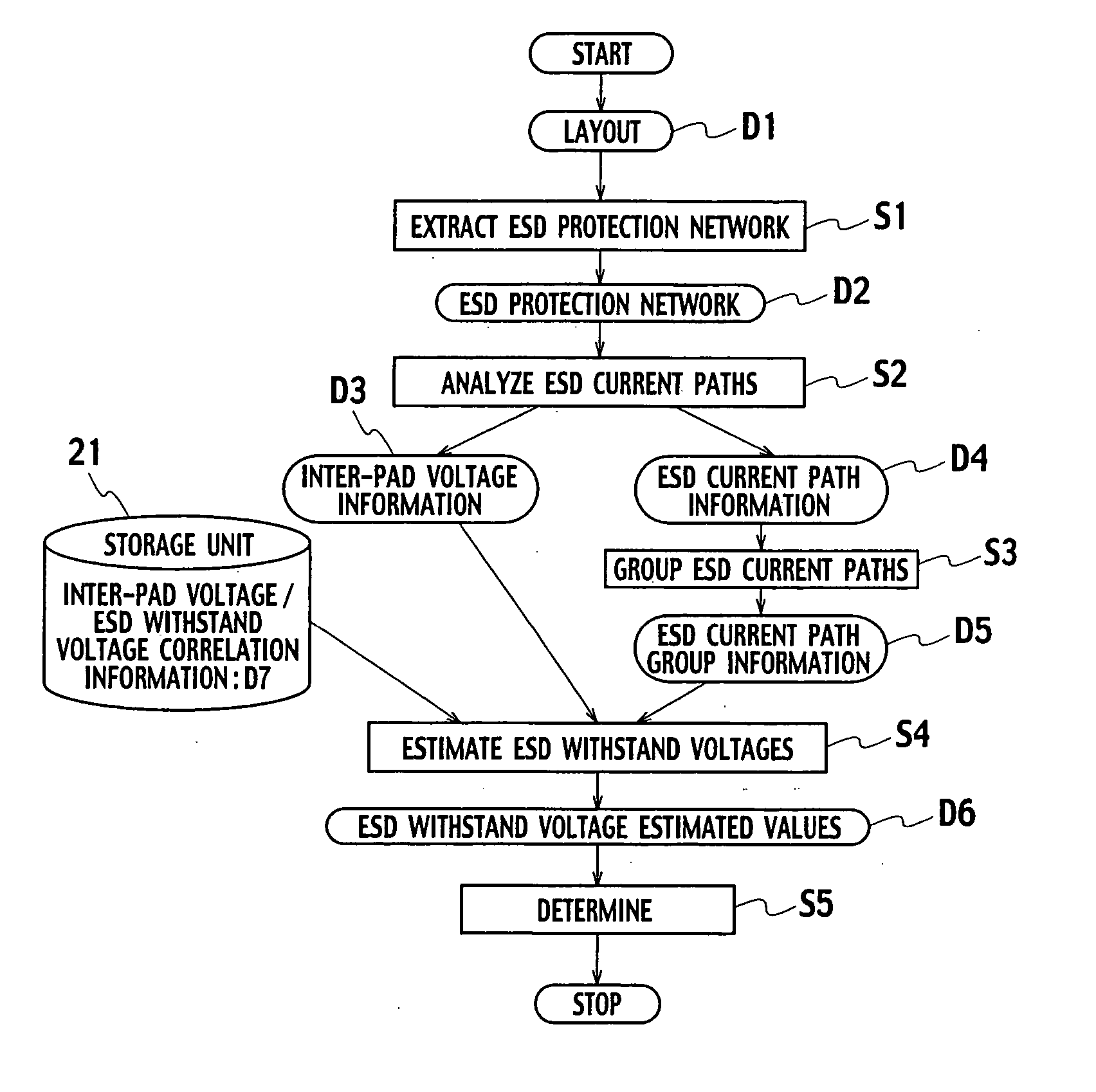
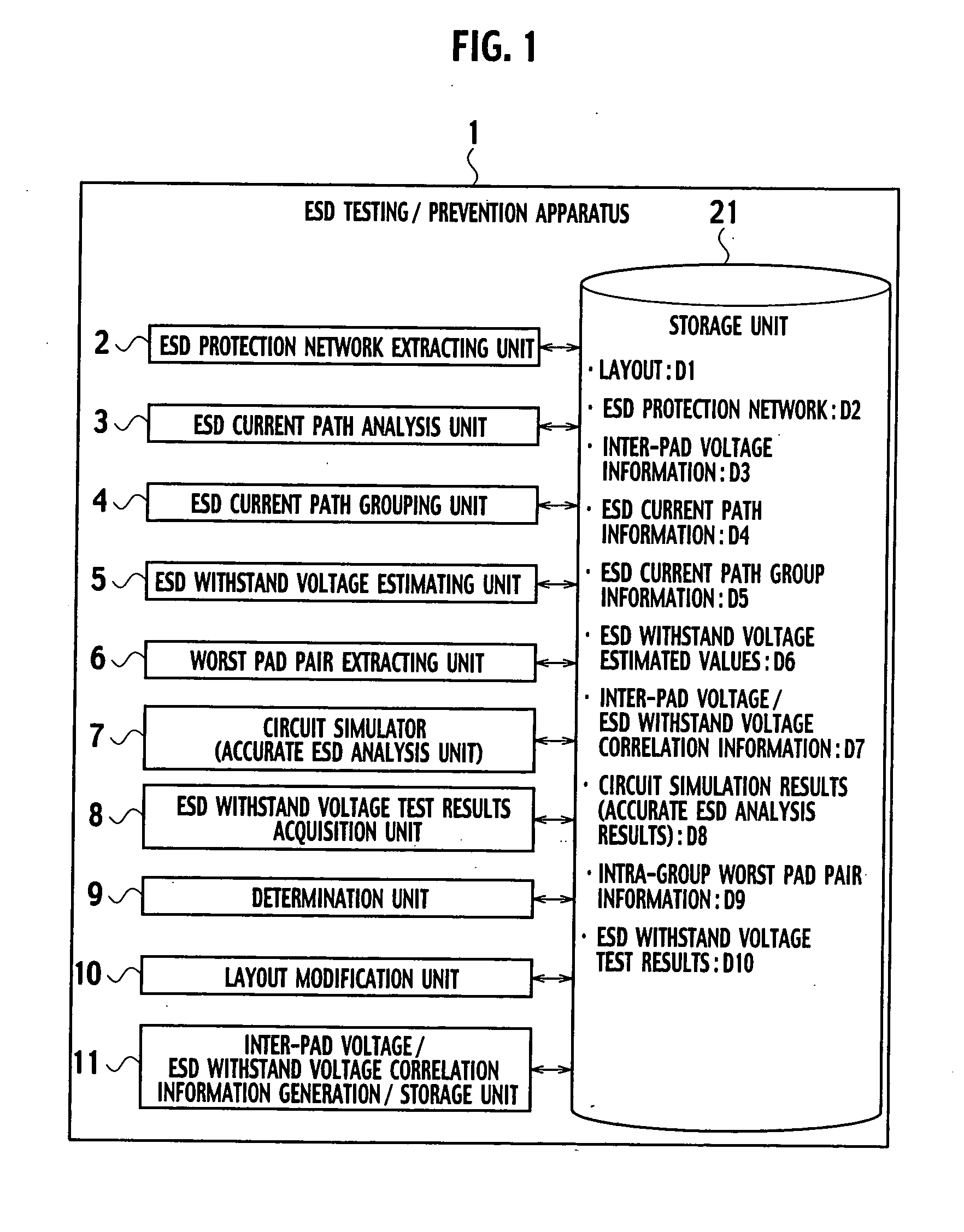
[0054] As shown in FIG. 1, an ESD testing / prevention apparatus 1 according to the first embodiment includes an ESD protection network extracting unit 2, an ESD current path analysis unit 3, an ESD current path grouping unit 4, an ESD withstand voltage estimating unit 5, a worst pad pair extracting unit 6, a circuit simulator (accurate ESD analysis unit) 7, an ESD withstand voltage test results acquisition unit 8, a determination unit 9, a layout modification unit 10, an inter-pad voltage / ESD withstand voltage correlation information generation / storage unit 11, and a storage unit 21. The storage unit 21 stores a layout D1, an ESD protection network D2, inter-pad voltage information D3, ESD current path information D4, ESD current path group information D5, ESD withstand voltage estimated values D6, inter-pad voltage / ESD withstand voltage correlation information D7, circuit simulation results (accurate ESD analysis results) D8, intra-group worst pad pair information D9, and ESD withst...

second embodiment

[0093] An ESD testing method according to the second embodiment may be implemented by the ESD testing / prevention apparatus of FIG. 1. As shown in FIG. 27, processing in steps S1 through S3, according to the ESD testing method of the second embodiment, is the same as that of the first embodiment shown in FIG. 2. With the ESD testing method of the second embodiment, after the step S3, processing in step S8 is carried out.

[0094] Furthermore, the ESD testing method according to the second embodiment differs from that according to the first embodiment in that the inter-pad voltage / ESD withstand voltage correlation information D7 is not needed. This is because the ESD current path set 15, generated in the step S2 as shown in FIG. 28A, is the same as that of FIG. 7. However, as shown in FIG. 28B, ESD withstand voltages are not directly used in ESD testing. Instead, virtual ESD withstand voltages may be used for the Y-axis in a distribution graph for ESD current paths with inter-pad voltag...

third embodiment

[0100] An ESD testing method according to the third embodiment may be implemented by the ESD testing / prevention apparatus of FIG. 1. As shown in FIG. 32, processing in steps S1 through step S3 and S8, according to the ESD testing method of the third embodiment, is the same as that of the second embodiment shown in FIG. 27. With the ESD testing method of the third embodiment, after the step S8, processing step S10 is carried out. Since processing according to the ESD testing method of the third embodiment also includes the step S8, measurement of ESD withstand voltages that correspond to all respective ESD current paths is unnecessary.

[0101] Up until the step S8, ESD withstand voltage testing is carried out for the paired start pad and end pad having the highest inter-pad voltage along each of the ESD current paths P1m, P2m, and P3b in each of the ESD current path groups G1 through G3, finding actual measurements of ESD withstand voltages.

[0102] In step S10, the ESD withstand volta...


PUM


Abstract

A method for determining a layout which passes testing for electrostatic discharge in a semiconductor device, includes extracting an electrostatic discharge protection network including pads, nets and protective elements; setting start pads and end pads in the electrostatic discharge protection network; finding inter-pad voltages between the start pads and the end pads and electrostatic discharge current paths from the start pads to the end pads; grouping together the electrostatic discharge current paths in the same order; calculating estimated values of electrostatic discharge withstand voltages between the start pads and the end pads and groups to which the start pads and the end pads belong using a negative correlation between the inter-pad voltages and corresponding electrostatic withstand voltages; and determining whether the layout passes testing regarding electrostatic discharge.

Description

CROSS REFERENCE TO RELATED APPLICATIONS AND INCORPORATION BY REFERENCE [0001] This application is based upon and claims the benefit of priority from the prior Japanese Patent Applications No. P2004-294961, filed on Oct. 7, 2004; the entire contents of which are incorporated herein by reference. BACKGROUND OF THE INVENTION [0002] 1. Field of the Invention [0003] The present invention relates to a testing method for electrostatic discharge of a semiconductor device. [0004] 2. Description of the Related Art [0005] A testing method of earlier technology for electrostatic discharge (ESD) of a semiconductor device includes extracting an ESD protection network from a layout of the semiconductor device, carrying out ESD current path analysis for a section of the network between two arbitrary pads using a shortest path search method to calculate an inter-pad voltage when an ESD current flows through an ESD current path, and determining the magnitude of an ESD withstand voltage based on the i...

Claims


Application Information

Patent Timeline
IPC IPC(8): H02H9/00
CPCG01R31/002G06F17/5036G06F30/367
Inventor HAYASHI, SACHIO
Owner KK TOSHIBA
Why Eureka
Try Eureka