
Method of forming conductive pattern

a technology of conductive pattern and conductive pattern, which is applied in the direction of nuclear engineering, transportation and packaging, railway signalling, etc., can solve the problems of inability to secure the conductive pattern with sufficient thickness, limited amount of ink, and inability to hold ink, etc., and achieves convenient formation, small width, and large thickness

Inactive Publication Date: 2006-05-25
SEIKO EPSON CORP
View PDF11 Cites 16 Cited by
  • Summary
  • Abstract
  • Description
  • Claims
  • Application Information

AI Technical Summary

Benefits of technology

[0007] An advantage of the invention is to provide a method of forming a conductive pattern. With the method, the conductive pattern can be easily formed so as to have a relatively large thickness and there is no landing mark even if the pattern has a smaller width than the landing diameter of the ink.
[0008] A method of forming a conductive pattern according to a first aspect of the invention includes a step of forming a bank on a substrate and a step of applying a lyophobic agent to a part or whole of an upper face of the bank.
[0009] According to the first aspect of the invention, the method includes the step of forming a bank on a substrate and the step of applying a lyophobic agent to a part or whole of an upper face of the bank. When the ink is discharged on the upper face of the bank by the ink-jet method, it can prevent the ink from remaining on the upper face of the bank with the lyophobic agent applied on a part or whole of an upper face of the bank. Accordingly, the conductive pattern that dose not have a landing mark on the bank upper face can be obtained.
[0010] A method of forming a conductive pattern according to a second aspect of the invention includes a step of forming a bank on a substrate, a step of giving a lyophilic quality to a part or whole of the substrate and the bank and a step of applying a lyophobic agent to a part or whole of an upper face of the bank.
[0011] According to the second aspect of the invention, it is possible to obtain a conductive pattern that dose not have a landing mark even if the width of the conductive pattern is smaller than a landing diameter of an ink.
[0012] In these cases, the lyophobic agent may be attached to an original plate member that is separately provided other than the substrate, and the lyophobic agent may be transferred to a part or whole of the upper face of the bank by contacting the original plate member with the upper face of the bank on the substrate.

Problems solved by technology

However, because of the lyophobic quality of the bank, only a limited amount of the ink could be held in the concave portion that is formed by the bank and the substrate.
Therefore, a sufficient thickness for the conductive pattern could not be secured and it was not appropriate as the conductive pattern though which a relatively large current passes.
Therefore, this became a problem impairing the electric credibility of the substrate.

Method used


Image

  • Method of forming conductive pattern
  • Method of forming conductive pattern
  • Method of forming conductive pattern

Examples


first embodiment

[0052] A first embodiment of the invention describes a process of forming a substrate and a bank on the substrate to which a method of forming a conductive pattern is applied, a process of giving lyophilicity to the substrate and a part or whole of bank, and a process of applying a lyophobic agent to a part or whole of an upper face of the bank.

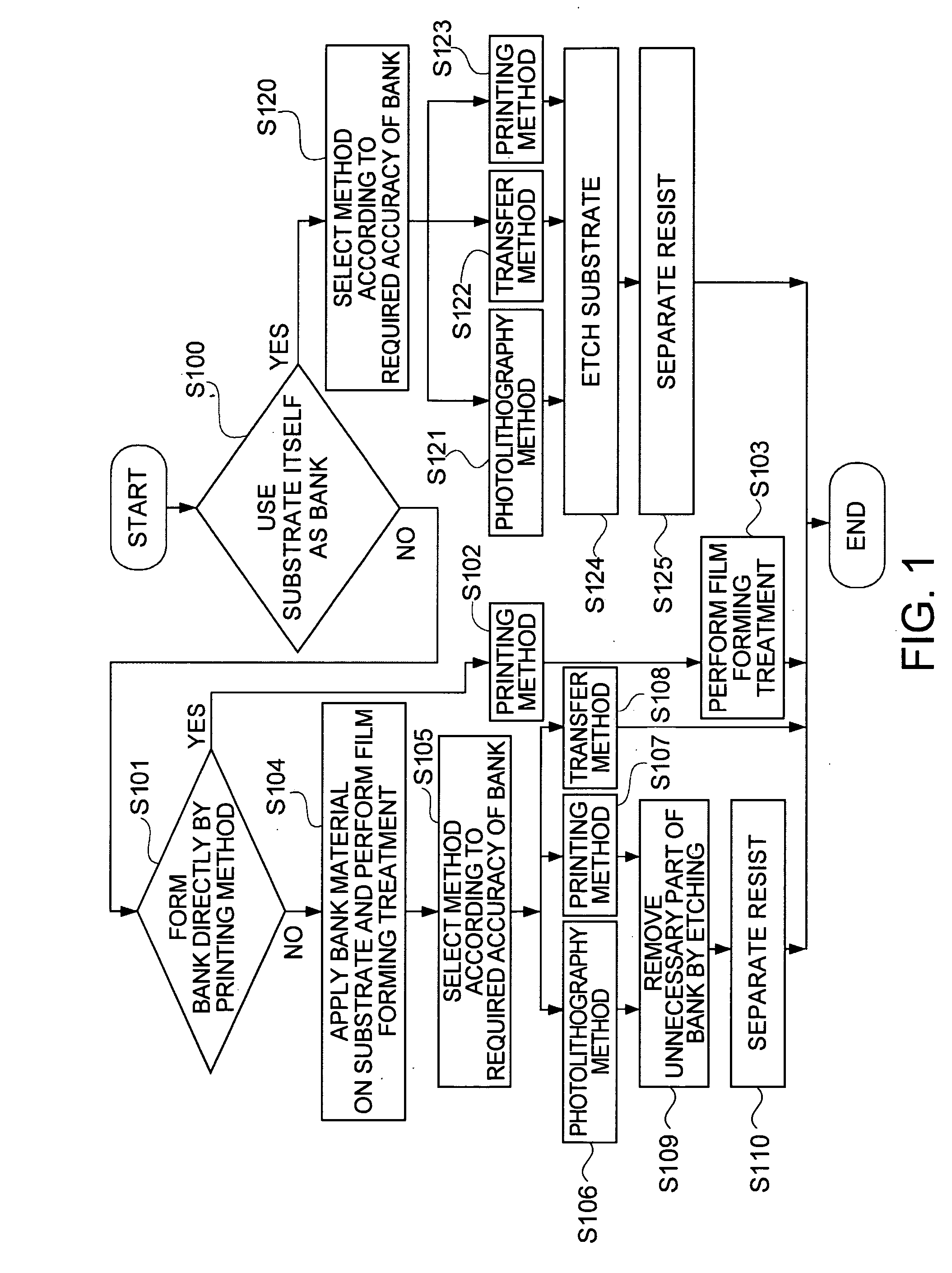
[0053] Flowchart of Process of Forming Substrate and Bank on the Substrate

[0054]FIG. 1 is a flow chart of a process of forming a substrate and a bank on the substrate. In this embodiment, whether the substrate itself is used as the bank or not will be chosen in Step (hereinafter denote as “S”) 100. When the substrate is not used as the bank, go to S101. When the substrate itself is used as the bank, go to S120.

[0055] As for the substrate, the following material can be used; transparent or translucent inorganic substrate materials such as glass and silica, monocrystal or non-monocrystal semiconductor substrate materials such as diamond, sil...

second embodiment

[0175] Next, a second embodiment is described with reference to the figures.

[0176] Only different parts from those of the first embodiment will be described in this embodiment and parts that are not described are the same as those of the first embodiment.

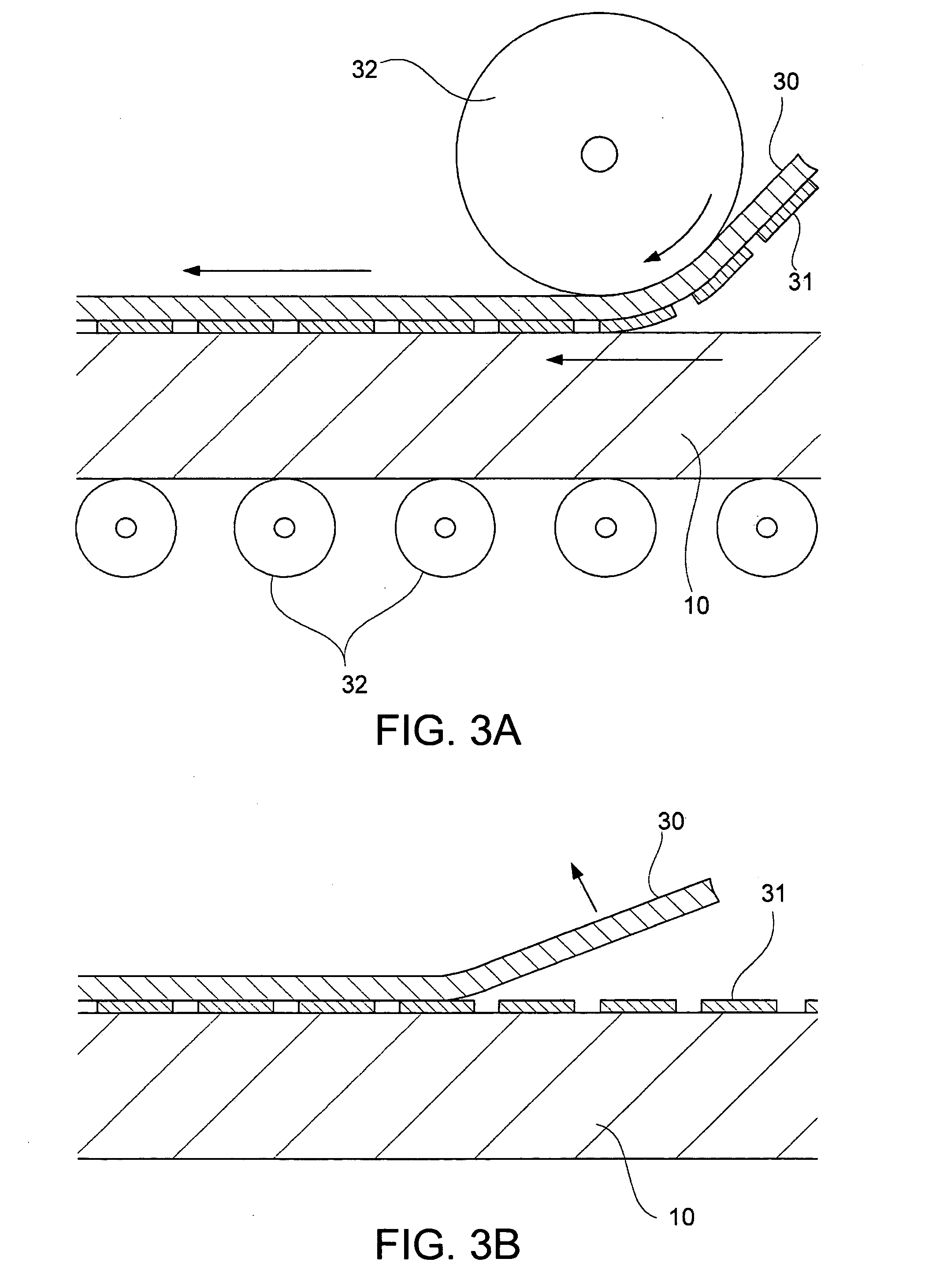
[0177]FIGS. 15A and 15B are a plan sectional view and a perspective view showing a process of forming a rolled original plate member 61.

[0178] A process of forming the rolled original plate member 61 which is a different member from the substrate 10 is described with reference to FIGS. 15A and 15B.

[0179] An inner wall 62a of the mold form 62 is processed with cylindrical grinding so as to have good roundness and cylindricality. A stepped opening 62b is provided under the mold form 62 so as to secure the same concentricity as that of the inner wall 62a. A bottom plate 64 having an opening 64a in its center is engaged with a bottom plate 63. The stamp material 54 described in the first embodiment is poured in the opening 64a.

[018...

third embodiment

[0185] Next, a third embodiment is described with reference to the figures.

[0186] Only different parts from those of the first embodiment will be described in this embodiment and parts that are not described are the same as those of the first embodiment.

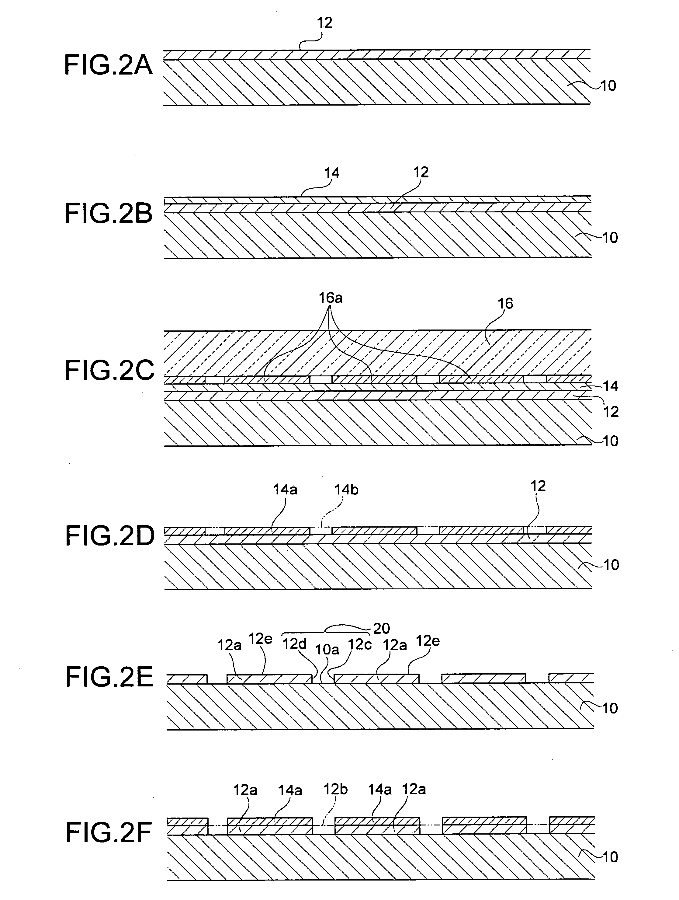
[0187] In this embodiment, the bank is formed by performing the emboss printing to the bank film 12 provided on the substrate 10 while the lyophobic agent 80 is applied. The necessary bank film 12a having a desired shape can be obtained and the process of giving the lyophobic quality to the bank upper face 12e is performed at the same time.

[0188]FIG. 16 is a sectional view of the substrate showing a process of applying the lyophobic agent 80 onto the bank upper face 12e of the necessary bank film 12a while forming the bank by the emboss printing method.

[0189] In FIG. 16, firstly, a film which becomes the bank film 12, for example, polymethylmethacrylate (PMMA) resin is formed on the substrate 10 as described above. Here, the bank...


PUM

PropertyMeasurementUnit
heightaaaaaaaaaa
contact angleaaaaaaaaaa
shrinkageaaaaaaaaaa

Abstract

A method of forming a conductive pattern includes a step of forming a bank on a substrate and a step of applying a lyophobic agent to a part or whole of an upper face of the bank.

Description

BACKGROUND OF THE INVENTION [0001] 1. Technical Field [0002] The present invention relates to a process of manufacturing a metal wiring by an ink-jet method. [0003] 2. Related Art [0004] JP-A-2002-305077 is an example of related art. As described in the example, a pattern of a partition wall member (hereinafter called a bank) which is a convexity formed on a substrate has been miniaturized by employing the ink-jet method. The bank has a lyophobic quality and the substrate has a lyophilic quality so that a conductive material liquid (hereinafter called an ink) discharged by the ink-jet method can settle in a concave portion (hereinafter called a bank groove part) which is formed by the bank and the substrate, and this can prevent the ink from flowing out of the bank. [0005] In a case of forming a conductive pattern through which a relatively large current passes, the pattern should be formed so as to have a certain thickness in order to reduce an electric resistance of the pattern. H...

Claims


Application Information

Patent Timeline
Patent Type & Authority Applications(United States)
IPC IPC(8): G21H5/00B05D3/00C08J7/18B32B3/10
CPCH01L21/288Y10T428/24273H01L27/3295H01L51/0022H05K3/125H05K3/1258H05K2201/09909H05K2203/013H05K2203/0568H05K2203/1173H01L2924/0002H01L21/76838H01L27/1292H01L2924/00H10K59/122H10K59/173H10K71/611H05B33/10H05B33/26
Inventor TOYODA, NAOYUKI
Owner SEIKO EPSON CORP
Features
  • Generate Ideas
  • Intellectual Property
  • Life Sciences
  • Materials
  • Tech Scout
  • Unparalleled Data Quality
  • Higher Quality Content
  • 60% Fewer Hallucinations
Learn More