

High surface area aluminum bond pad for through-wafer connections to an electronic package
- Summary
- Abstract
- Description
- Claims
- Application Information
AI Technical Summary
Benefits of technology
Problems solved by technology
Method used
Image

Examples
Embodiment Construction
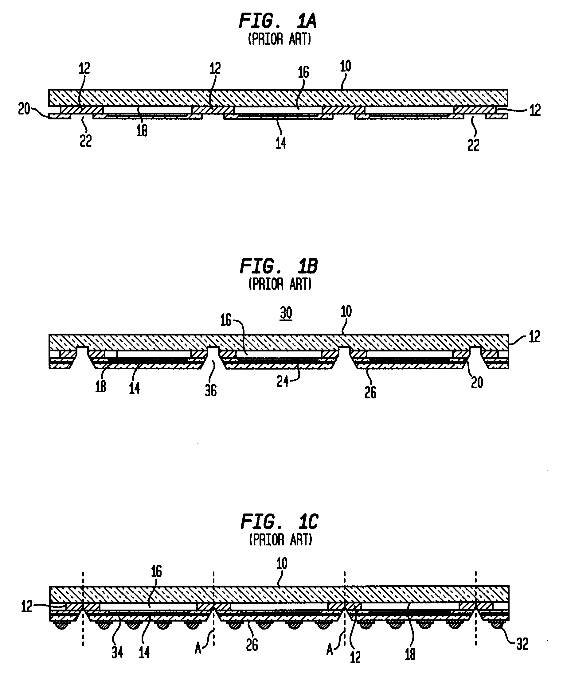
[0018] Referring to FIGS. 1A through 1C of the drawings, setting forth a prior art example of producing an electronic package, this is directed to a process for forming through-wafer connections by etching a via through the backside of a wafer and through bond pads, so as to expose the edges of the pads.
[0019] Hereby, as shown in FIG. 1A of the drawings, a front glass plate 10 has a plurality of spacer rims 12 attached thereto, and a die 14 is located to form a cavity 16 between the backside 18 of the front glass plate 10 and a silicon pad 20, etches 22 are implemented from the backside of the die so as to form I / Os (inputs / outputs) to the die. Thereafter, as shown in FIG. 1B of the drawings, a layer of glue 24 is employed to attach a back glass plate 26, and notching at angles to a normal is implemented for forming the initial structure 30 prior to singulation (by dicing).
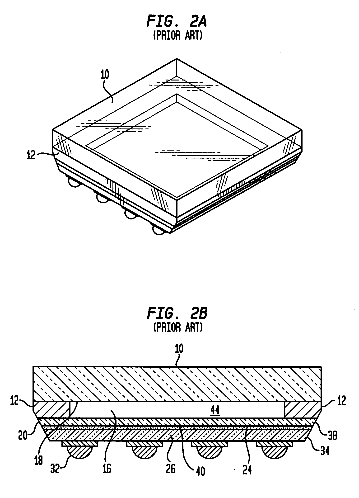
[0020] Thereafter, as shown in FIG. 1C of the drawings, BGA solder bumps 32 are suitably fastened to the back...
PUM
 Abstract
Description
Claims
Application Information