Multivariate control of semiconductor processes

Active Publication Date: 2006-05-25
SARTORIUS STEDIM DATA ANALYTICS AB
View PDF21 Cites 61 Cited by
  • Summary
  • Abstract
  • Description
  • Claims
  • Application Information

AI Technical Summary

Benefits of technology

[0021] In another aspect, the invention features a system for simultaneously detecting and classifying a fault condition of a manufacturing process. The system includes means for acquiring data associated with a plurality of manufacturing related variables for a plurality of outputs of a manufacturing process and means for acquiring fault class data associated with the outputs of the manufacturing process. The system also includes means for developing a model based on the data and the fault class data for detecting faulty

Problems solved by technology
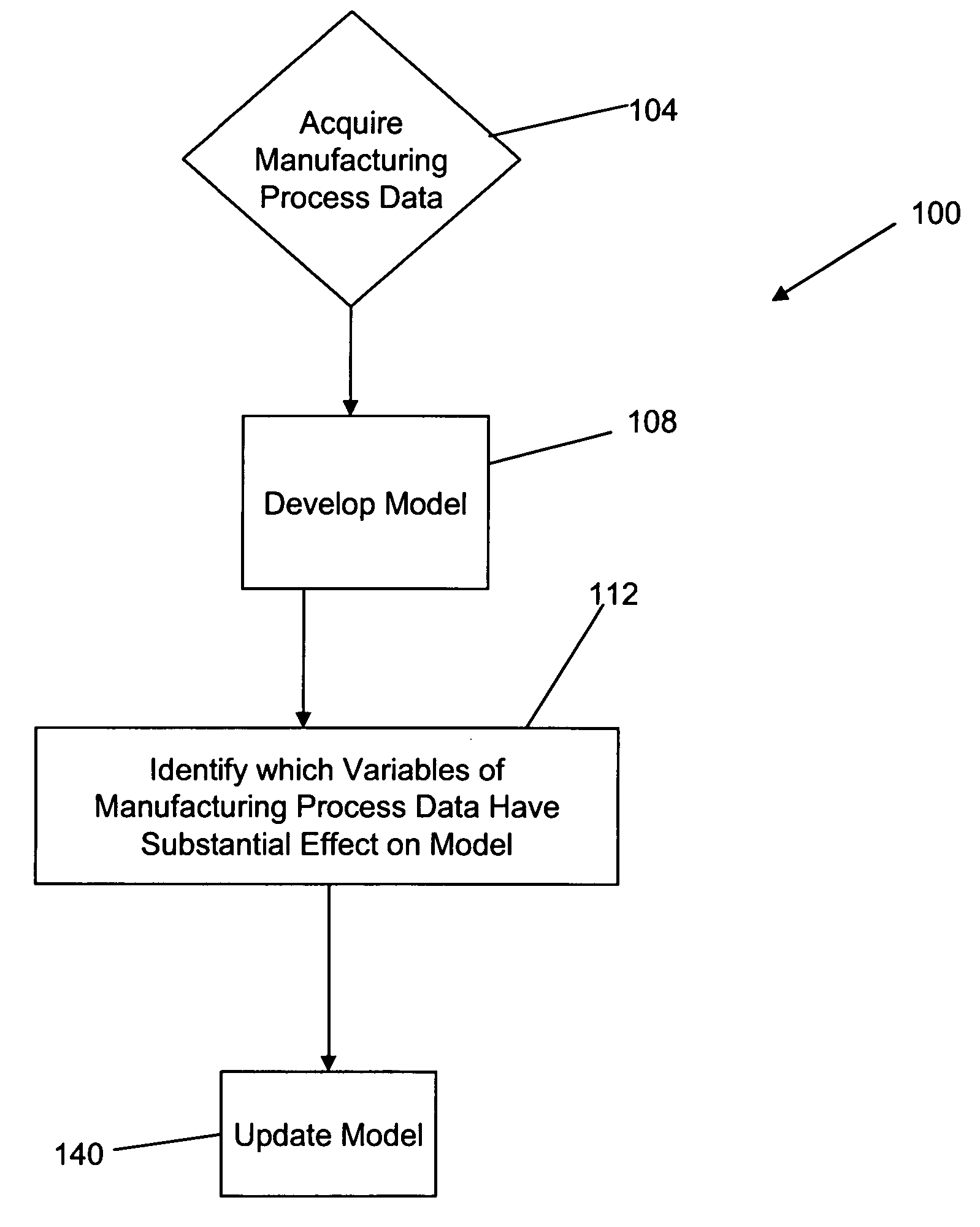
As device geometries shrink to the nanometer scale, however, the increasing complexity of manufacturing processes has changed the landscape that must be negotiated to meet and maintain process/materials specifications.
Stand-alone control of process tools (based on equipment state data) will not maintain viable yields at 65 and 45 nm.
Furthermore, tool level control alone cannot meet all of the control needs of advanced device fabrication.
The cost of purchasing (and developing) stand-alone process tools to meet advanced production specifications is expected to be staggering.
It seems surprising that AEC/APC is not already widely implemented, given such strong driving forces.
However, significant obstacles to AEC/APC exis

Method used


Image

  • Multivariate control of semiconductor processes
  • Multivariate control of semiconductor processes
  • Multivariate control of semiconductor processes

Examples


Example

EXAMPLE

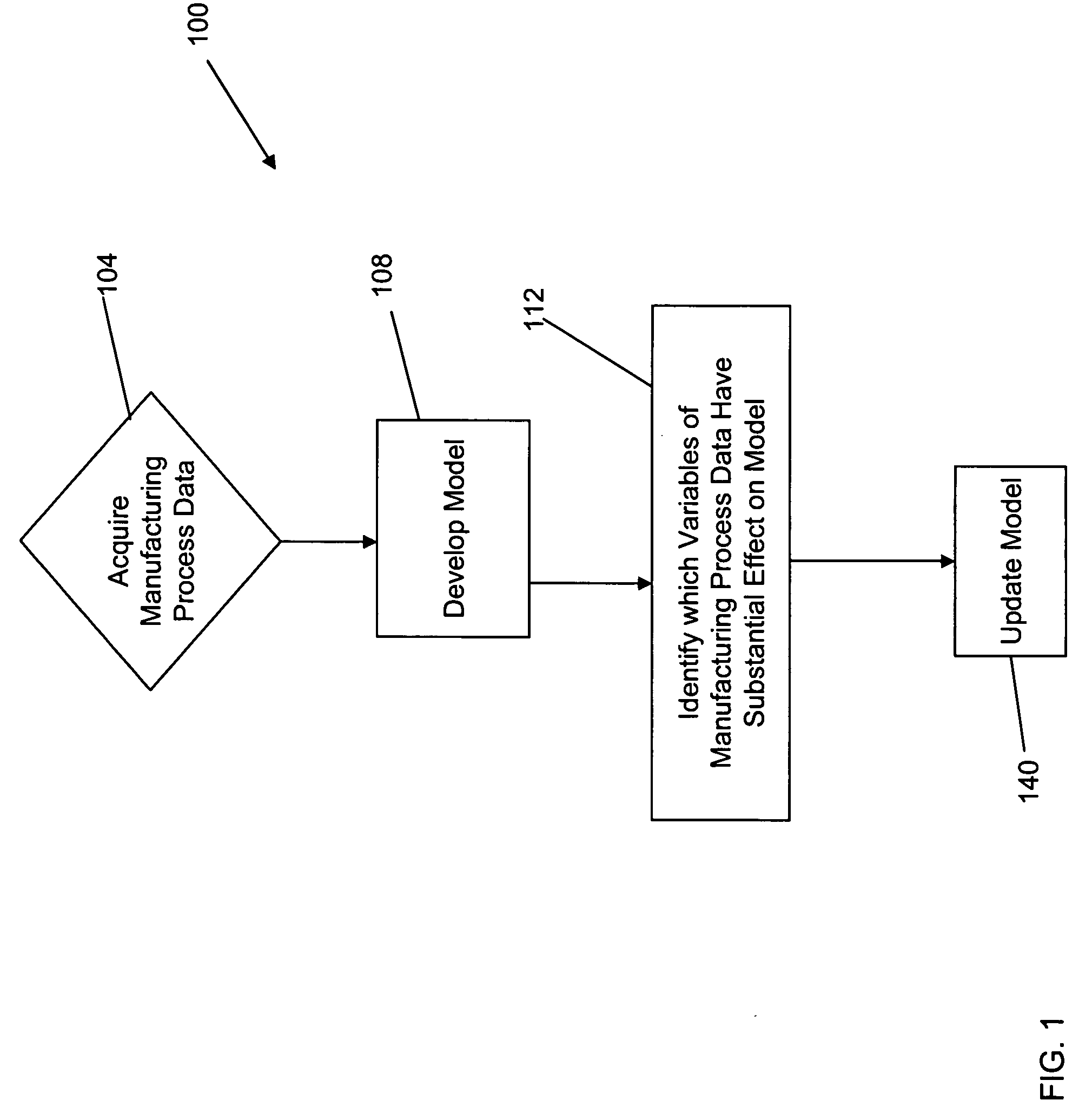
[0054] By way of illustration, an experiment was conducted to detect faulty wafers (wafers having photoresist located on the surface of the wafer) of a semiconductor fabrication process. In this experiment, 24 wafers were output by the manufacturing process. Of the 24 wafers, 19 of the wafers (wafers 1, 2, 4, 5, 6, 8, 9, 11, 12, 13, 14, 16, 17, 19, 20, 21, 22, 23, and 24) have no photoresist material located on the surface of the wafer. Wafers 3, 7, 10, 15, and 18 have photoresist on the surface of the wafer.

[0055] A residual gas analysis (RGA) was conducted on the wafers to acquire the RGA spectra from 2 AMU through 80 AMU (79 different measurements) for each of the wafers. EQN. 1 was used to format the manufacturing data, the matrix X has K=79 columns (79 measurements for each of 2 AMU through 80 AMU) and N=19 rows (19 wafers corresponding to all the non-photoresist wafers). As described previously herein, the matrix X was then scaled (the average of each column of the ma...


PUM


Abstract

A method for detecting a fault condition of a manufacturing process involving acquiring data and developing a model based on a plurality of manufacturing related variables for a plurality of outputs of a manufacturing process. The method also involves identifying which of the manufacturing related variables have a substantial affect on the model for detecting faulty outputs of the manufacturing process. The method also involves updating the model by using the manufacturing related variables identified as having a substantial affect on the model to improve the ability of the model to detect faulty outputs of the manufacturing process.

Description

RELATED APPLICATIONS [0001] This application claims priority to U.S. provisional application Ser. No. 60 / 611,136, filed on Sep. 17, 2004, and entitled “Multivariate Control of Semiconductor Processes.”FIELD OF THE INVENTION [0002] The present invention relates to methods and apparatus for detecting fault conditions of manufacturing processes and classifying fault types associated with outputs of manufacturing processes. BACKGROUND OF THE INVENTION [0003] Historically, semiconductor device manufacturers have managed the transition to tighter process / materials specifications by depending on process tool manufacturers to design better and faster process / hardware configurations. As device geometries shrink to the nanometer scale, however, the increasing complexity of manufacturing processes has changed the landscape that must be negotiated to meet and maintain process / materials specifications. [0004] Stand-alone control of process tools (based on equipment state data) will not maintain ...

Claims


Application Information

Patent Timeline
IPC IPC(8): G06F19/00
CPCG05B19/4184G05B2219/31357G05B2219/45031Y02P90/02Y02P90/80
Inventor LIN, KUO-CHIN
Owner SARTORIUS STEDIM DATA ANALYTICS AB
Why Eureka
Try Eureka