Method and process for design of integrated circuits using regular geometry patterns to obtain geometrically consistent component features

Active Publication Date: 2006-05-25
PDF SOLUTIONS INC
View PDF6 Cites 219 Cited by
  • Summary
  • Abstract
  • Description
  • Claims
  • Application Information

AI Technical Summary

Benefits of technology

[0011] The invention provides a method and process for designing an integrated circuit based on using the results from both 1) a specific set of silicon test structure characterizations and 2) the decomposition of logic into combinations of simple logic primitives, from which a set of logic bricks are derived that can be assembled for a manufacturable-by-construction design. This implementation of logic is compatible with the lithography settings that are used

Problems solved by technology

It is important to note that the logic gates are designed without regular geometry pattern constraints, and their boundaries with neighboring cells in the final layout are not constrained for prin

Method used


Image

  • Method and process for design of integrated circuits using regular geometry patterns to obtain geometrically consistent component features
  • Method and process for design of integrated circuits using regular geometry patterns to obtain geometrically consistent component features
  • Method and process for design of integrated circuits using regular geometry patterns to obtain geometrically consistent component features

Examples


Embodiment Construction

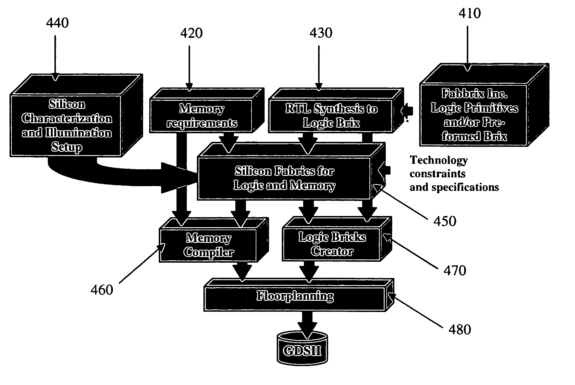
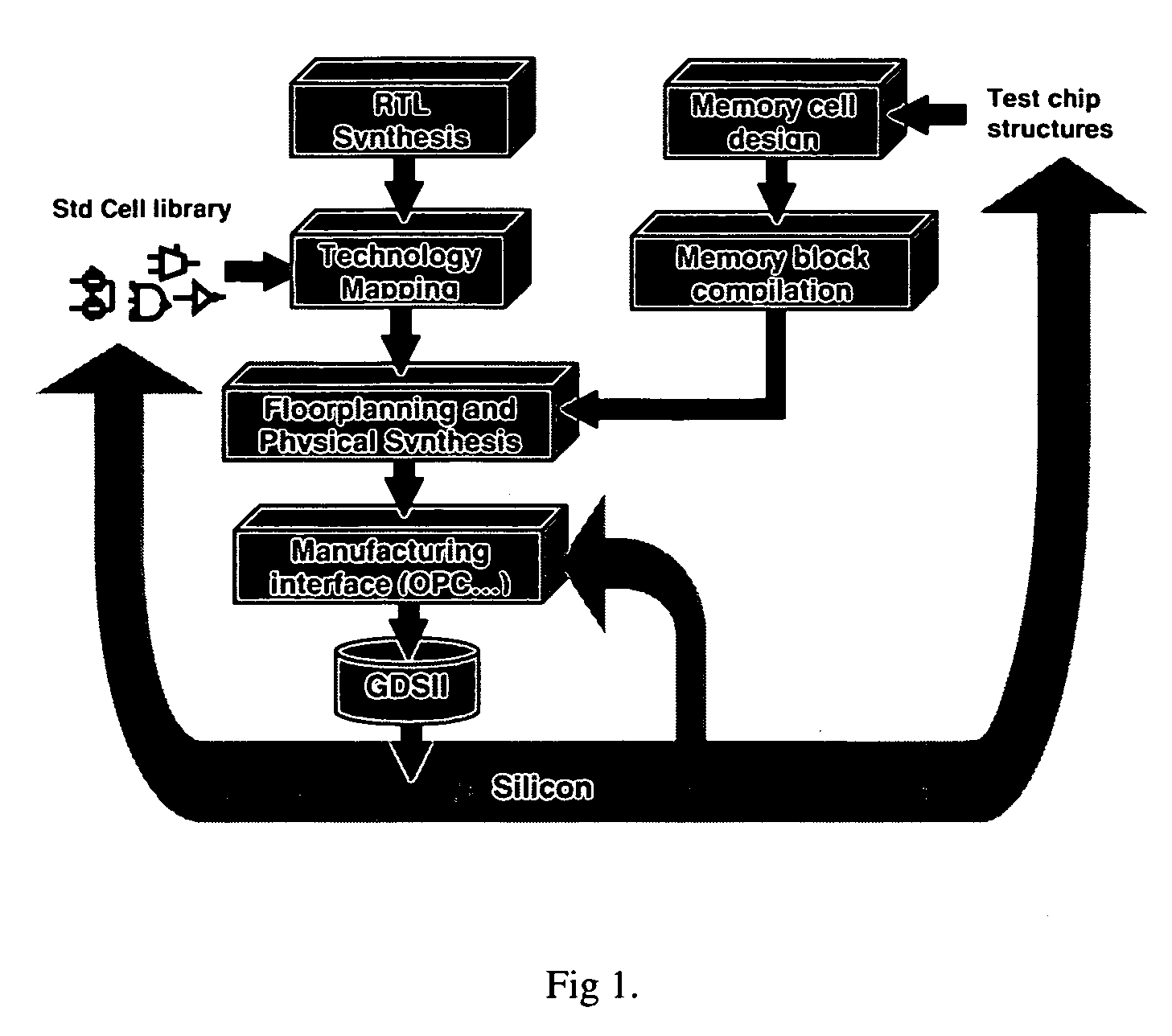
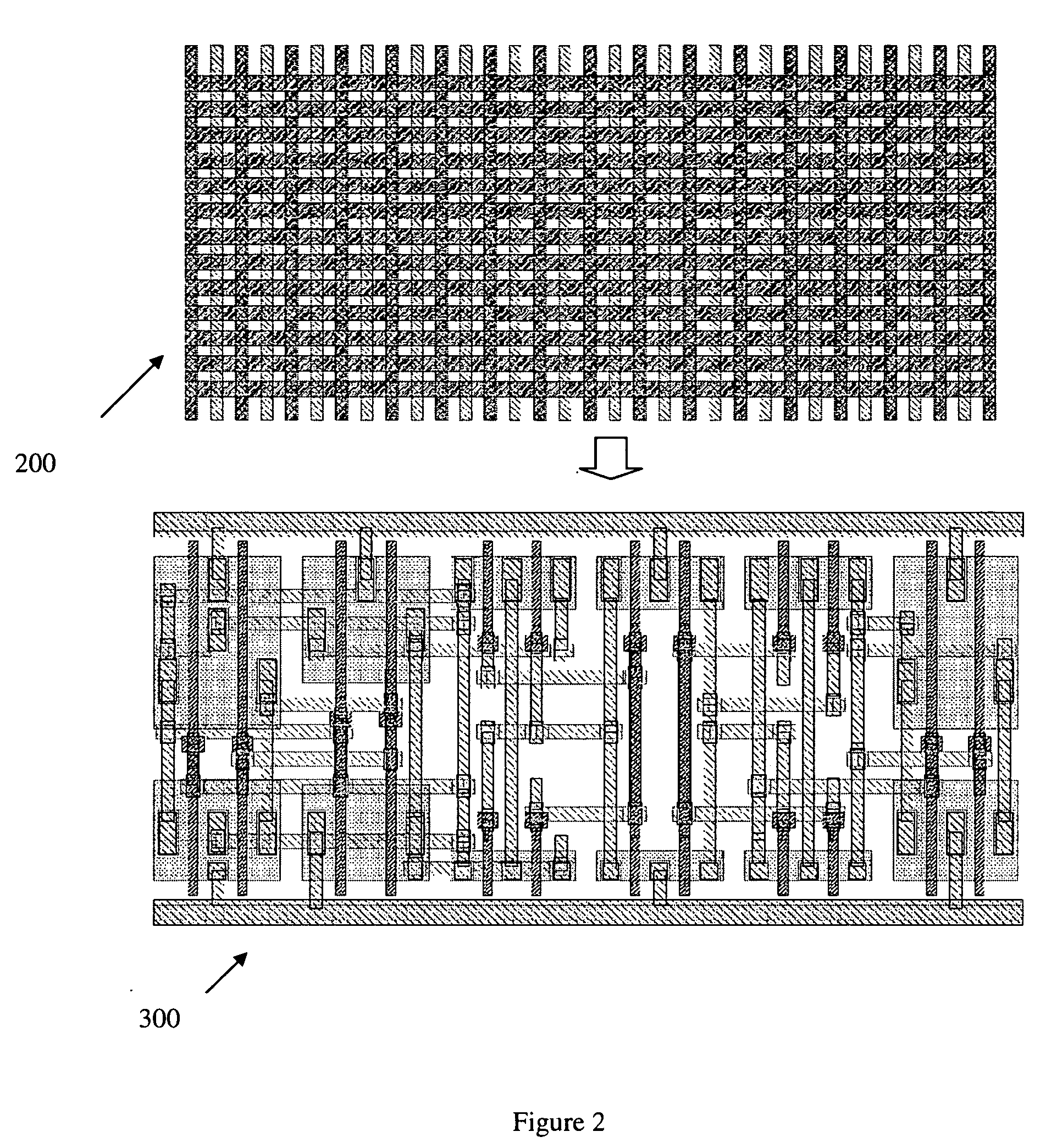
[0017] This invention provides a method and process by which silicon test structures are first fabricated to define uniform patterns of geometrical shapes. These uniform patterns of geometrical shapes are used to define the underlying fabric from which the component features for the electronic devices and associated interconnect structures on the integrated circuit are derived such that they are geometrically consistent, preferably for a specific lithography setup. The invention provides a means whereby these uniform patterns of geometrical shapes (also referred to as regular patterns, or regular geometrical patterns) will be optimized to match the corresponding settings for the illumination controls that will be used for lithography. The invention also provides a novel method and means by which illumination controls are determined by the requirements of the uniform pattern printing, as well as the printing of the geometrical patterns for memory cells and other integrated circuit co...


PUM


Abstract

The invention provides a method and process for designing an integrated circuit based on using the results from both 1) a specific set of silicon test structure characterizations and 2) the decomposition of logic into combinations of simple logic primitives, from which a set of logic bricks are derived that can be assembled for a manufacturable-by-construction design. This implementation of logic is compatible with the lithography settings that are used for implementation of the memory blocks and other components on the integrated circuit, particularly by implementing geometrically consistent component features. The invention provides the ability to recompile a design comprised of logic and memory blocks onto a new geometry fabric to implement a set of technology-specific design changes, without requiring a complete redesign of the entire integrated circuit.

Description

PRIORITY CLAIM [0001] This application claims priority to U.S. Provisional Application No. 60 / 625,342 entitled “A Method and Process for Design of Integrated Circuits Using Regular Geometry Patterns” filed on Nov. 4, 2004, and which is expressly incorporated by reference herein.BACKGROUND [0002] 1. Field of the Invention [0003] The present invention relates to a method and process for design of integrated circuits using regular geometry patterns to obtain component features that are geometrically consistent and, more particularly to the design of integrated circuits that have memory cells and logic components using regular geometry patterns to obtain geometrically consistent component features. [0004] 2. Background of the Invention [0005] The active devices (transistors) and metal interconnecting layers for an integrated circuit (IC) are typically created by printing geometrical shapes onto a mask, then using a lithography process to translate said shapes onto layers of materials th...

Claims


Application Information

Patent Timeline
IPC IPC(8): G06F17/50
CPCG06F17/5068G06F30/39
Inventor PILEGGI, LAWRENCE T.STROJWAS, ANDRZEJ J.LANZA, LUCIO L.
Owner PDF SOLUTIONS INC
Why Eureka
Try Eureka