Eureka AIR delivers breakthrough ideas for toughest innovation challenges, trusted by R&D personnel around the world.

Method for reducing wafer charging during drying

a technology of electrostatic charging and drying, applied in the field of photolithography techniques, can solve the problems of increasing the particle contamination increasing the density of finished chips or dies fabricated on the wafer, and increasing the electrostatic charge of the wafer surface, so as to reduce the formation of defects in devices fabricated, prevent or reduce electrostatic interference with processing equipment, and eliminate or reduce the accumulation of electrostatic charges

Inactive Publication Date: 2006-06-01
TAIWAN SEMICON MFG CO LTD
View PDF5 Cites 13 Cited by
  • Summary
  • Abstract
  • Description
  • Claims
  • Application Information

AI Technical Summary

Benefits of technology

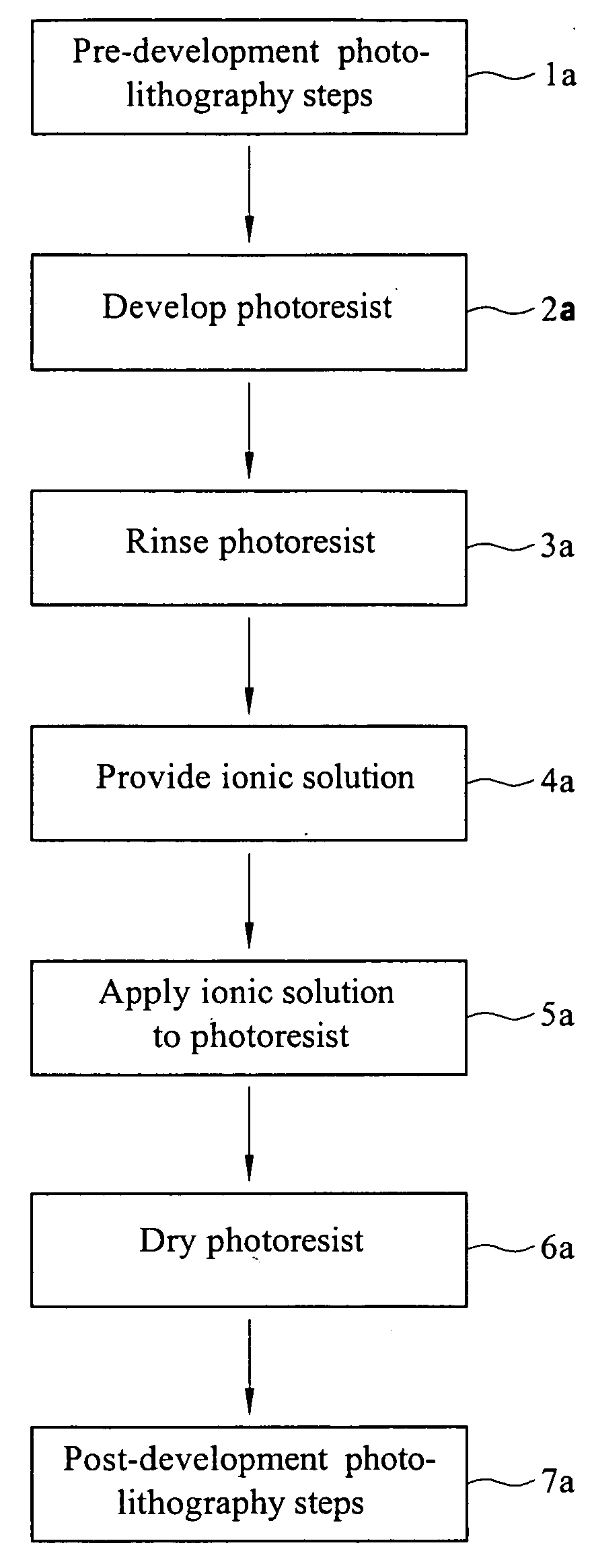
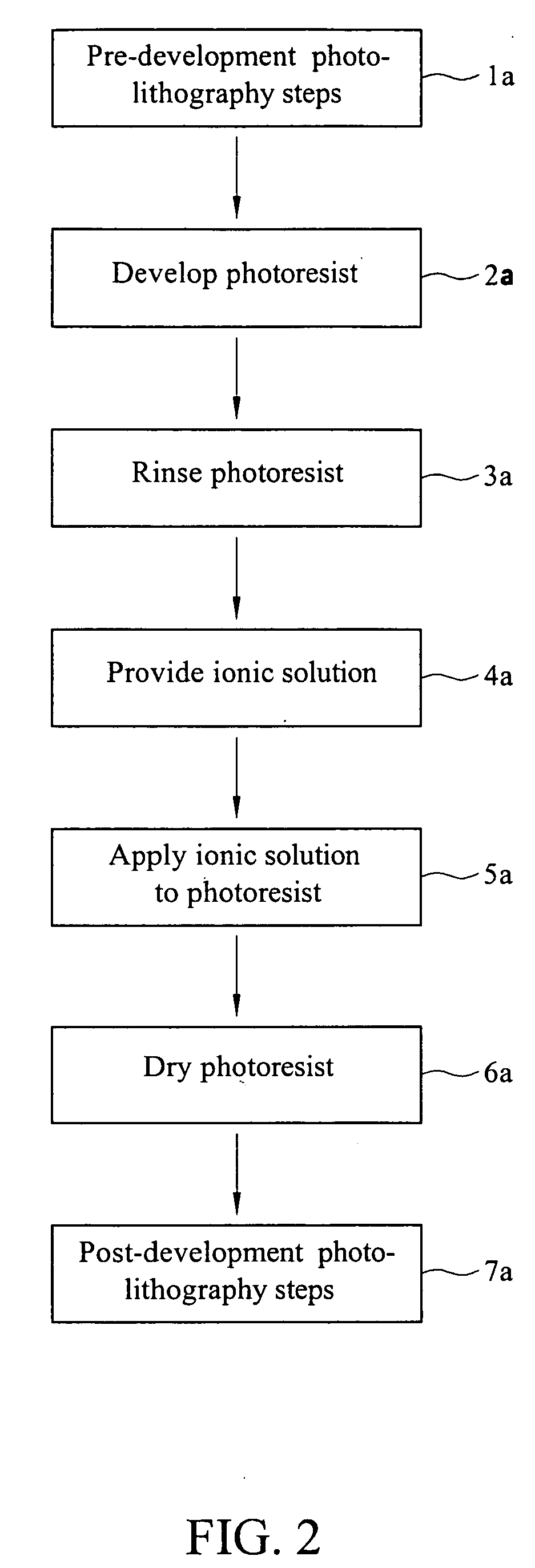
[0016] In accordance with these and other objects and advantages, the present invention is generally directed to a novel method for eliminating or reducing the accumulation of electrostatic charges on semiconductor wafers during spin-rinse-drying of the wafers in the fabrication of integrated circuits (ICs), particularly during photolithography. The method includes rinsing a wafer; applying an ionic solution to the wafer; and spin-drying the wafer. During the spin-drying step, the ionic solution neutralizes electrostatic charges on the wafer as the wafer is rotated. This reduces the formation of defects in devices fabricated on the wafer, as well as prevents or reduces electrostatic interference with processing equipment during photolithographic and other fabrication processes. The ionic solution can be either acidic or alkaline. Preferably, the ionic solution has a pH of typically about 6˜10.

Problems solved by technology

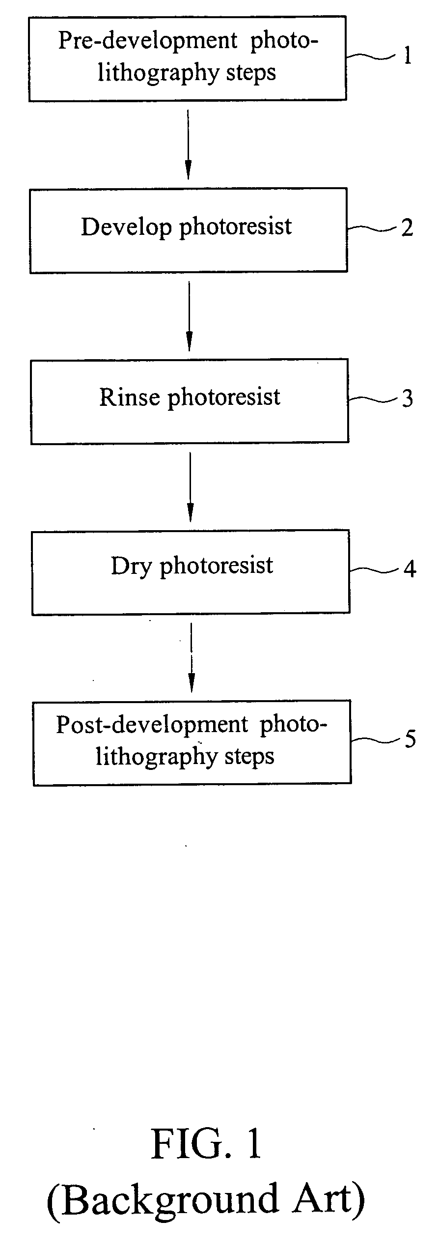
One of the limitations of the SRD drying step is that rotation of the wafer frequently results in electrostatic charging of the wafer surface.
The presence of electrostatic charges on the surface of the wafer increases particle contamination of the wafer surface.
This ultimately leads to defect densities in the finished chips or die fabricated on the wafer, as revealed by chip testing.
Furthermore, electrostatic charges on the surface of the wafer frequently interferes with the operation of production equipment, thus decreasing up-time, interrupting process flow or requiring re-processing of the semiconductor products.
The problems caused by electrostatic charges tend to be more of a problem in photolithography areas than in other areas of semiconductor production.

Method used


Image

  • Method for reducing wafer charging during drying
  • Method for reducing wafer charging during drying
  • Method for reducing wafer charging during drying

Examples


Embodiment Construction

[0023] The present invention contemplates a novel method for eliminating or at least reducing the accumulation of electrostatic charges on semiconductor wafers during spin-rinse-drying of the wafers in the fabrication of integrated circuits (ICs), particularly during the photolithography stage of semiconductor fabrication. According to the method, a wafer is initially rinsed typically in a spin-rinse-dry (SRD) module. An ionic solution is then applied to the wafer, which is then subjected to a spin-drying step. During the spin-drying step, the ionic solution neutralizes electrostatic charges on the rotating wafer. Consequently, electrostatic attraction of particles to the wafer is reduced. This, in turn, reduces the formation of defects in devices fabricated on the wafer. Furthermore, electrostatic interference with processing equipment during photolithographic and other fabrication processes is eliminated or at least substantially reduced.

[0024] The ionic solution applied to the w...


PUM

PropertyMeasurementUnit
diameteraaaaaaaaaa
acidicaaaaaaaaaa
alkalineaaaaaaaaaa

Abstract

A novel method for eliminating or reducing the accumulation of electrostatic charges on semiconductor wafers during spin-rinse-drying of the wafers is disclosed. The method includes rinsing a wafer; applying an ionic solution to the wafer; and spin-drying the wafer. During the spin-drying step, the ionic solution neutralizes electrostatic charges on the wafer as the wafer is rotated. This reduces the formation of defects in devices fabricated on the wafer, as well as prevents or reduces electrostatic interference with processing equipment during photolithographic and other fabrication processes.

Description

FIELD OF THE INVENTION [0001] The present invention relates to photolithography techniques used in the fabrication of integrated circuits on semiconductor wafer substrates. More particularly, the present invention relates to a novel method for reducing electrostatic charging of wafers during photolithography, particularly during spin rinse drying of wafers after photolithography development, by applying an ionic solution to the wafers prior to the spin rinse drying step. BACKGROUND OF THE INVENTION [0002] The fabrication of various solid state devices requires the use of planar substrates, or semiconductor wafers, on which integrated circuits are fabricated. The final number, or yield, of functional integrated circuits on a wafer at the end of the IC fabrication process is of utmost importance to semiconductor manufacturers, and increasing the yield of circuits on the wafer is the main goal of semiconductor fabrication. After packaging, the circuits on the wafers are tested, wherein...

Claims


Application Information

Patent Timeline
Patent Type & Authority Applications(United States)
IPC IPC(8): G03F7/00
CPCG03F7/405H01L21/02057
Inventor WANG, YU-HSIWANG, SHI-CHELIN, HUA-TALHO LIN, SHANGCHANG, CHING-YULIN, CHIN-HSIANG
Owner TAIWAN SEMICON MFG CO LTD
Why Eureka
Eureka Blog
Learn More