Eureka AIR delivers breakthrough ideas for toughest innovation challenges, trusted by R&D personnel around the world.

Fluxes effective in suppressing non-wet-open at bga assembly

a technology of fluxes and assemblies, applied in the field of fluxes, can solve the problems of increasing thermal warpage, increasing the challenges of board assembly, and introducing additional defects into the reflow solder process, and achieve the effect of reducing or eliminating non-wet open (nwo) defect formation

Active Publication Date: 2019-12-05
INDIUM CORPORATION
View PDF0 Cites 1 Cited by
  • Summary
  • Abstract
  • Description
  • Claims
  • Application Information

AI Technical Summary

Benefits of technology

This patent describes a system and method for preventing defects in semiconductor packaging called non-wet open (NWO) by using a low activity flux to prevent solder paste from sticking to solder balls during reflow soldering. The low activity flux coating the solder ball prevents the formation of a NWO, which is a common problem in semiconductor packaging. This technology improves the reliability and quality of semiconductor packaging.

Problems solved by technology

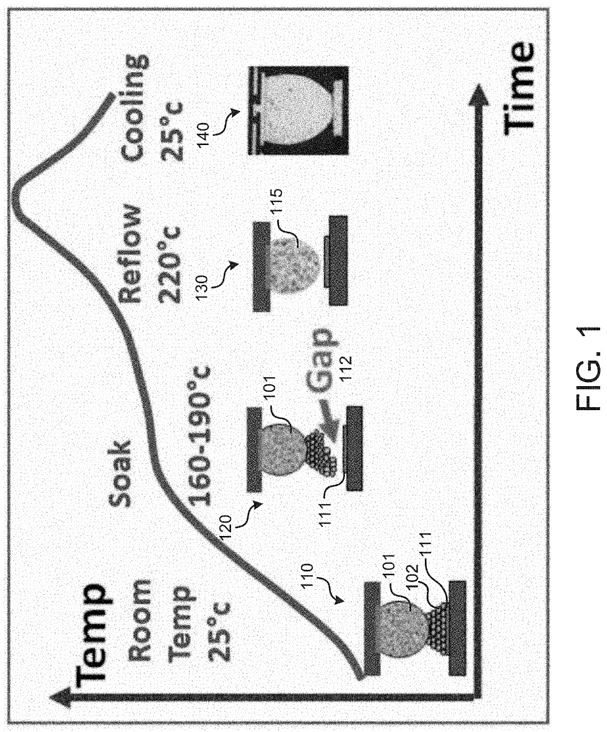
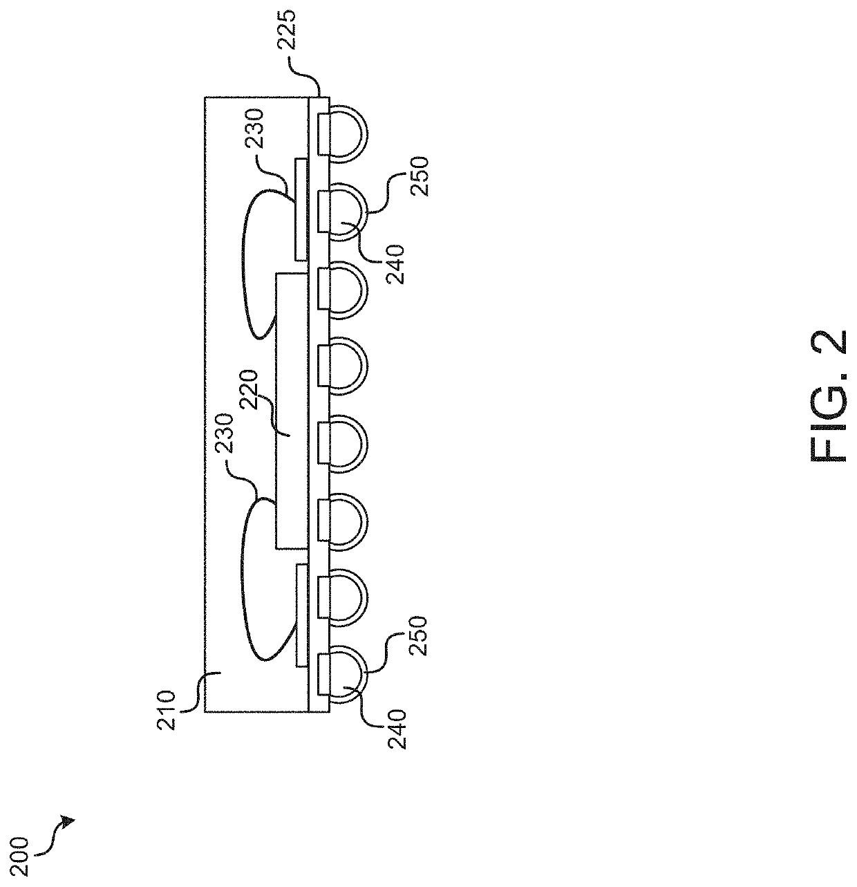
Due to a coefficient of thermal expansion (CTE) mismatch between the die and molding compound of the BGA, this is increasing thermal warpage during reflow processing.
These trends in the industry are increasing the challenges of board assembly and introducing additional defects into the reflow solder process.
One defect that has increased in incidence (e.g., due to a CTE mismatch) is the formation of a non-wet-open (NWO) defect at the BGA.
As the temperature of the assembly is heated, the shape of the BGA may begin to warp (e.g., due to a mismatch of the CTEs between the die and molding compound of the BGA).
This lifting of paste 102 may subsequently cause a NWO defect.
Additionally the exposed PCB pad 111 may exposed to a high reflow temperature, causing it to grow oxides that impede wetting.

Method used


Image

  • Fluxes effective in suppressing non-wet-open at bga assembly
  • Fluxes effective in suppressing non-wet-open at bga assembly
  • Fluxes effective in suppressing non-wet-open at bga assembly

Examples


Embodiment Construction

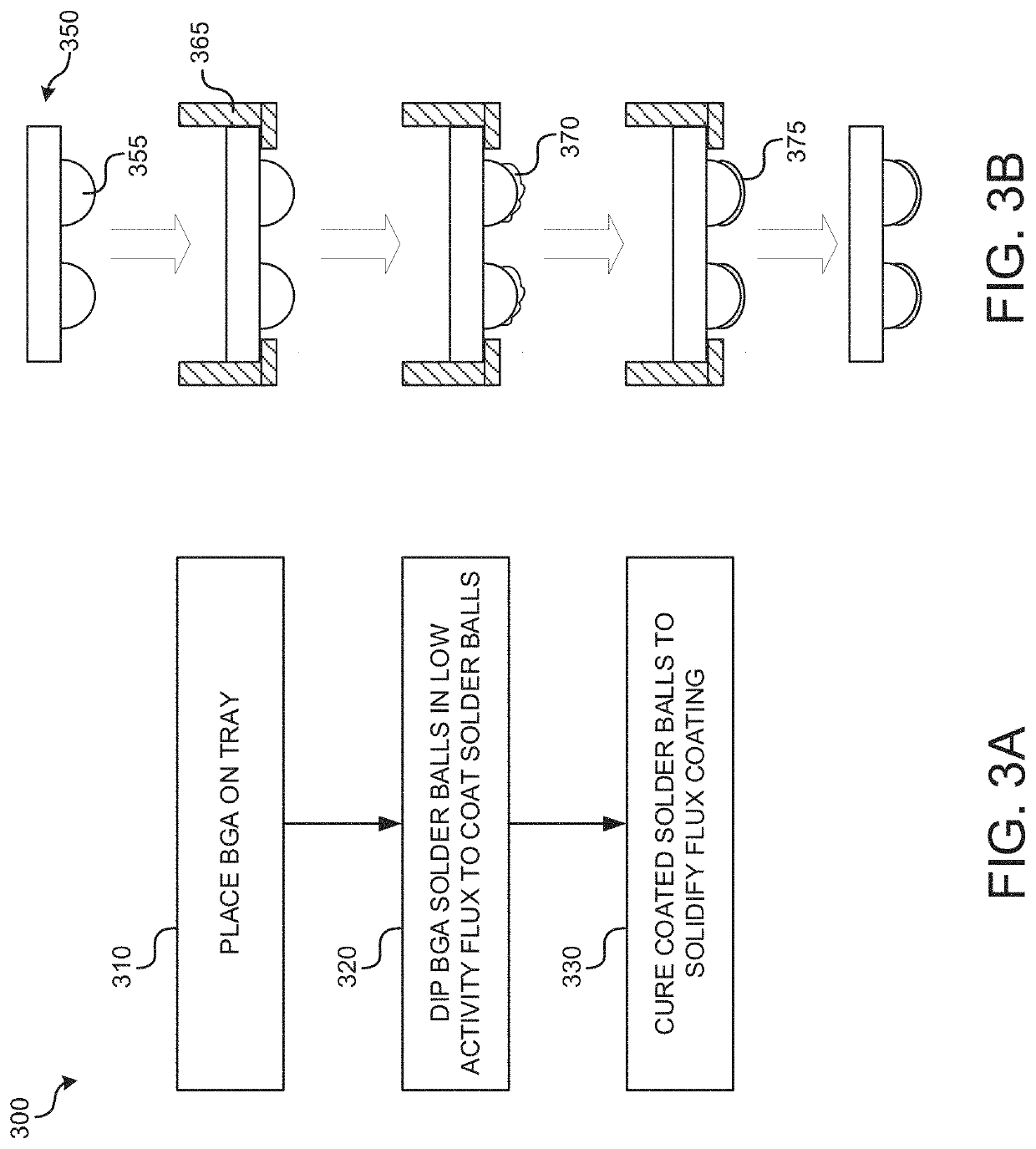
[0008]Systems and methods are described for eliminating or reducing non-wet open (NWO) defect formation by using a low activity flux to prevent a solder paste from sticking to ball grid array (BGA) solder balls during reflow soldering.

[0009]In one embodiment, a method includes: dispensing solder paste on a pad of a printed circuit board (PCB); mounting a ball grid array (BGA) on the PCB to form an assembly, where mounting the BGA on the PCB includes mounting a flux coated solder ball of the BGA on the dispensed solder paste, where the flux is a low activity flux; and reflow soldering the assembly to form a solder joint, where during reflow, the low activity flux coating the solder ball prevents the formation of a non-wet open between the solder joint and the pad, where the solder paste reflows into the solder ball to form the solder joint. During reflow, a flux of the solder paste dispensed on the PCB may penetrate through the low activity flux to remove oxides and promote wetting o...


PUM


Abstract

The disclosure describes techniques for eliminating or reducing non-wet open (NWO) defect formation by using a low activity flux to prevent a solder paste from sticking to ball grid array (BGA) solder balls during reflow soldering. The low activity flux may be configured such that: i) it creates a barrier that prevents the solder paste from sticking to the solder balls of the BGA; and ii) it does not impede the formation of solder joints during reflow. In implementations, a solid coating of the low activity flux may be formed over balls of the BGA, and the BGA may then be bonded to a PCB during reflow. In implementations, the balls of a BGA may be dipped in a low-activity creamy or liquid flux prior to reflow. In some implementations, the flux may applied on a solder paste printed on pads of the PCB, followed by placement of a BGA.

Description

CROSS REFERENCE TO RELATED APPLICATIONS[0001]This application claims priority to Chinese Patent Application No. 201810553189.5, filed on May 31, 2018.TECHNICAL FIELD[0002]The present disclosure relates generally to ball grid arrays.DESCRIPTION OF THE RELATED ART[0003]A ball grid array (BGA) is a surface-mount package that may be used to permanently mount and electrically connect components on a surface of printed circuit boards (PCBs). In a BGA, balls (sometimes referred to as “bumps”) of solder may be placed in a grid pattern on a substrate on an underside of the package. The PCB onto which the BGA is mounted may have a matching set of metal pads (e.g., copper pads) for receiving the solder balls to provide electrical interconnection.[0004]With the continuing miniaturization of electronic components, the die of the BGA is getting thinner and the solder balls are getting smaller. Additionally, environmentally friendly manufacturing is driving the use of Pb-free solders, which increa...

Claims


Application Information

Patent Timeline
IPC IPC(8): H01L23/00H05K3/34
CPCH01L24/17H01L2924/15311H05K3/3436H01L24/11B23K35/3613H01L23/3128H05K13/0465B23K35/0244B23K35/025B23K35/3612B23K35/3615B23K35/362H05K3/3489H05K2201/10734H05K2203/0485
Inventor ZHOU, FENGYINGCHEN, FENLEE, NING-CHENG
Owner INDIUM CORPORATION
Why Eureka
Eureka Blog
Learn More