Method of manufacturing semiconductor device to decrease defect number of plating film

a technology of plating film and semiconductor, which is applied in the direction of semiconductor devices, basic electric elements, electrical appliances, etc., can solve the problems of reducing device features, reducing device performance, and narrowing of cu wiring width, so as to reduce the defect number of plated films after cmp, and reduce the defect number of films

Inactive Publication Date: 2008-11-20
RENESAS ELECTRONICS CORP
View PDF12 Cites 3 Cited by
  • Summary
  • Abstract
  • Description
  • Claims
  • Application Information

AI Technical Summary

Benefits of technology

[0056]Also when the reverse bias step is inserted in the middle of the first electroplating step (that is, a fine-pattern filling step), the impurity is incorporated into the plated film. Nevertheless, since a wiring width filled is small, an influence of the impurity to the film becomes large too much. In consequence, there arises a problem that wiring resistance rises. In addition, since even the suppressor which exists on a surface of the plated film is removed, film quality becomes less precise and a defect number increases. On the other hand, in the case of the field film forming step, a wiring width is wide, and since the impurity is incorporated moderately, the reduction effect of the defect number in the plated film after CMP is obtained. Hence, in this embodiment, the reverse bias step is not inserted in the middle of the electroplating step of filling a fine-pattern at the first current density.
[0065]In addition, at the reverse bias step, when a current density at the reverse bias step is high and time is long since a plated film is electrolytically etched, time necessary to form a desired film thickness becomes long, and hence, throughput decreases. For this reason, it is preferable that the current density and time in reverse bias are set at minimum values necessary for an accelerator being emitted into and resolved in a plating solution.
[0066]In the above-mentioned description, the current density means a value obtained by dividing an anode current value by a substrate area. In addition, a step of performing entering into a bath with applying a constant voltage before the first electroplating step may be included. The voltage here may be between a cathode and an anode, or may be a voltage between a reference electrode and the cathode, in a plating solution The voltage in the step of performing entering into a bath is set so as to become a current density in the range of 0.1 to 6 A / dm2.
[0067]Defects of a Cu plated film after CMP are classified roughly into defects resulting from poor Cu plating filling, and defects formed at a subsequent heat treatment step and CMP step. The defects formed at a post step are caused by film quality of a plated film, a stress in the plated film, a type of a CMP drug solution, and the like.
[0068]On the other hand, it is known that a carbon impurity in a Cu film suppresses vacancy cluster formation under a stress. The defects formed at the post step are suppressed and reduced by vacancy cluster formation. Although a mechanism by which vacancy cluster formation is suppressed by an impurity is not solved, it is conceivable as follows. That is, when being given heat treatment after plating, Cu expands thermally, but since it is not completely resilient, volume of a Cu film after heat treatment becomes smaller than that before the heat treatment, and hence, an internal stress is generated. A carbon impurity in a film stabilizes a grain boundary by depositing in a grain boundary, and limits diffusion of a hole due to the internal stress. In consequence, formation of a vacancy cluster is suppressed. Although it becomes possible to reduce defect formation caused by a stress because of a high impurity concentration, this is considered to be an advantageous effect which relieves an influence by the stress.
[0070]In this embodiment, a plating solution can be made to be the same as that of what contains a suppressor and an accelerator and is used for forming a plated film at the time of normal copper wiring formation. The plating solution of this embodiment can further contain, for example, sulfuric acid, copper, or chlorine. In addition, the plating solution may also contain other additives such as a leveler.

Problems solved by technology

In recent semiconductor devices, the device performance has been limited by delay of signal propagation in wiring.
In addition, a Cu wiring width has also become narrow by decreasing device features following requests of high integration in recent years.
Therefore, a defect in a wiring layer results in not only increasing wiring resistance, but also disconnection, and seriously influences reliability of a semiconductor device.
Although being what prevented erosion and the like in a CMP step by inserting a reverse bias as a planarization step, conventional techniques had a task that there were still many defects in a plated film after the CMP step.
A defect here means a pit and chipping in a Cu wiring layer and a via.
This defect had an adverse effect on reliability of a semiconductor device.
Thereby, although flat property of a pattern may improve, there are still many defects in a plated film after CMP.
Although a reverse bias is similarly inserted once between a filling step and a field film forming step in Japanese Patent Laid-Open No. 2004-270028, the task that there are many defects in a plated film after CMP still remains.
Although it is disclosed that an increase in film thickness on a fine wiring pattern by the suppressor removal is effective for suppression of erosion, this poses a problem of causing a CMP cost increase and dishing.

Method used


Image

  • Method of manufacturing semiconductor device to decrease defect number of plating film
  • Method of manufacturing semiconductor device to decrease defect number of plating film
  • Method of manufacturing semiconductor device to decrease defect number of plating film

Examples


first embodiment

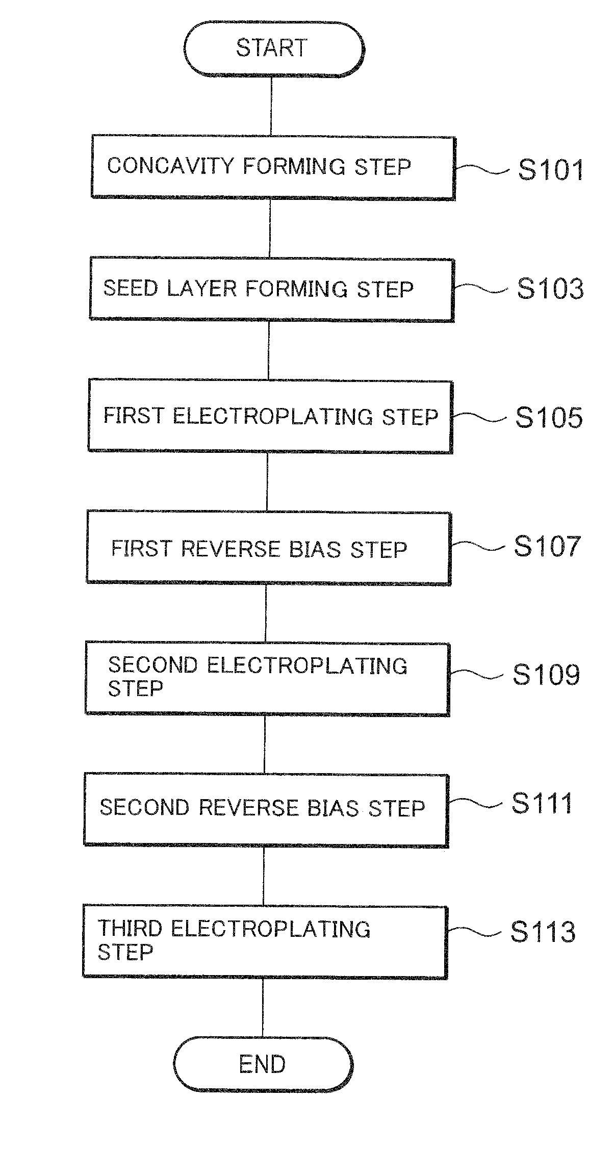
[0040]Hereafter, an embodiment of the present invention will be described with referring to FIGS. 1 to 3.

[0041]FIG. 1 is a flowchart for describing a method of manufacturing a semiconductor device in this embodiment. The method of manufacturing a semiconductor device in this embodiment has order of a concavity forming step (S101), a seed layer forming step (S103), a first electroplating step (S105), a first reverse bias step (S107), a second electroplating step (S109), a second reverse bias step (S111), and a third electroplating step (S113), and includes a series of these steps. In addition, a conceptual diagram of a current profile in each plating step is as illustrated in FIG. 3.

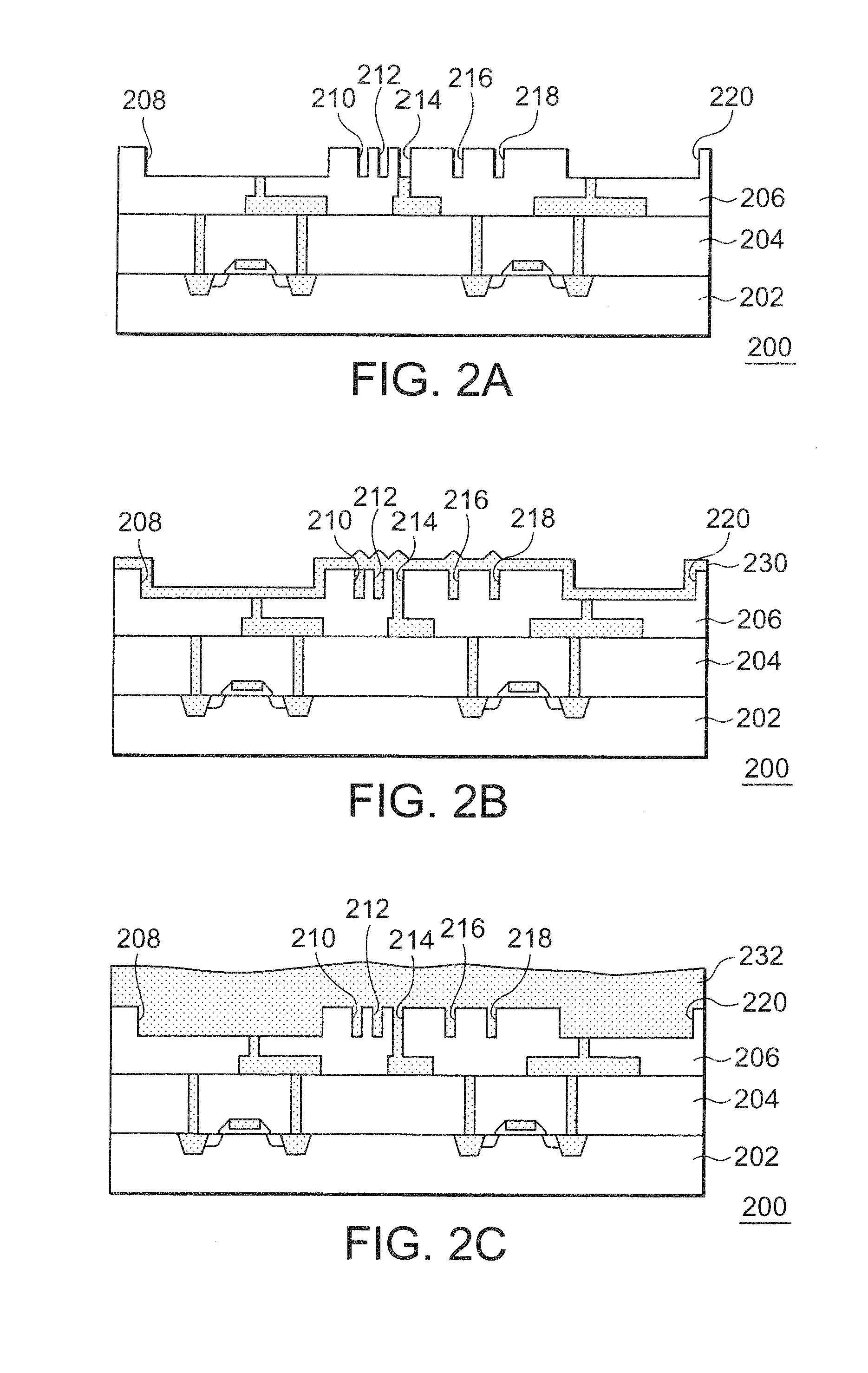
[0042]FIGS. 2A to 2C are step sectional views of illustrating steps of producing a semiconductor device 200 in this embodiment. In this embodiment, a step of forming wiring in an inter-layer insulating film 206 will be described. In FIG. 2, although procedure of forming copper wiring with taking a case of...

example 1

[0077]Cu electroplating was performed in a current profile (this is called a current profile C) illustrates in FIG. 4. In the current profile C, a first electroplating step of filling a fine pattern at a first current density (I1), a first reverse bias step of applying a current at the second current density (I2) after filling of the fine pattern is completed, a second electroplating step of using the third current density (I3), a second reverse bias step of applying a current at the same current density as the second current density (I2), and a third electroplating step of using the same current density as the third current density (I3) were performed successively.

[0078]Here, the first current density (I1) was set in a range of 0.2 A / dm2 to 1 A / dm2 inclusive. Here, in this specification, a current direction that goes to the cathode from an anode is defined as a positive direction. In addition, time of the first electroplating step was made 20 seconds to 200 seconds inclusive. The s...

second embodiment

[0085]A flowchart illustrating a method of manufacturing a semiconductor device in this embodiment and step sectional views expressing steps of producing the semiconductor device are the same as those of the first embodiment. However, it is different from the first embodiment at a point that an absolute value of an integrated current amount at a second reverse bias step is larger than an absolute value of an integrated current amount at a first reverse bias step. Thereby, the defect number in a plated film after a CMP step is further reduced. Hereinafter, this embodiment will be described with focusing on different points from the first embodiment.

[0086]FIG. 8 is a conceptual diagram illustrating a current profile in a plating step in this embodiment. A first electroplating step, a second electroplating step, and a third electroplating step are set as the same conditions as those in the first embodiment. Those preferable ranges are the same as those in the first embodiment. In this ...


PUM

PropertyMeasurementUnit
current densityaaaaaaaaaa
thicknessaaaaaaaaaa
widthaaaaaaaaaa

Abstract

A method for manufacturing a semiconductor device is provided which includes performing an electroplating step to fill concavities formed on a substrate. The electroplating step further includes: performing a first electroplating step; performing a first reverse bias step; performing a second electroplating step; performing a second reverse bias step; and a third electroplating step. The polarity of the first and the second reverse bias steps is different from that of the first electroplating step. A difference between the third current density and the fourth current density is larger than a difference between the first current density and the second current density.

Description

BACKGROUND OF THE INVENTION[0001]1. Field of the Invention[0002]The present invention relates to a method of manufacturing a semiconductor device. In particular, the present invention relates to a method of manufacturing a semiconductor device by which a defect number in wiring or a via which include a plating film is reduced.[0003]2. Description of the Related Art[0004]In recent semiconductor devices, the device performance has been limited by delay of signal propagation in wiring. A delay constant in wiring is expressed by product of wiring resistance and capacitance between wirings. In order to lower wiring resistance to accelerate device operation, Cu is usually used for a wiring material, because Cu has a small resistivity.[0005]In addition, a Cu wiring width has also become narrow by decreasing device features following requests of high integration in recent years. Therefore, a defect in a wiring layer results in not only increasing wiring resistance, but also disconnection, a...

Claims


Application Information

Patent Timeline
Patent Type & Authority Applications(United States)
IPC IPC(8): C25D5/18
CPCC25D5/18C25D7/123H01L21/76877H01L21/2885
Inventor FURUYA, AKIRAKOZUMI, SHINSUKEARITA, KOJI
Owner RENESAS ELECTRONICS CORP
Why Eureka
Try Eureka