

Programmable device
- Summary
- Abstract
- Description
- Claims
- Application Information
AI Technical Summary
Benefits of technology
Problems solved by technology
Method used
Image

Examples
first embodiment
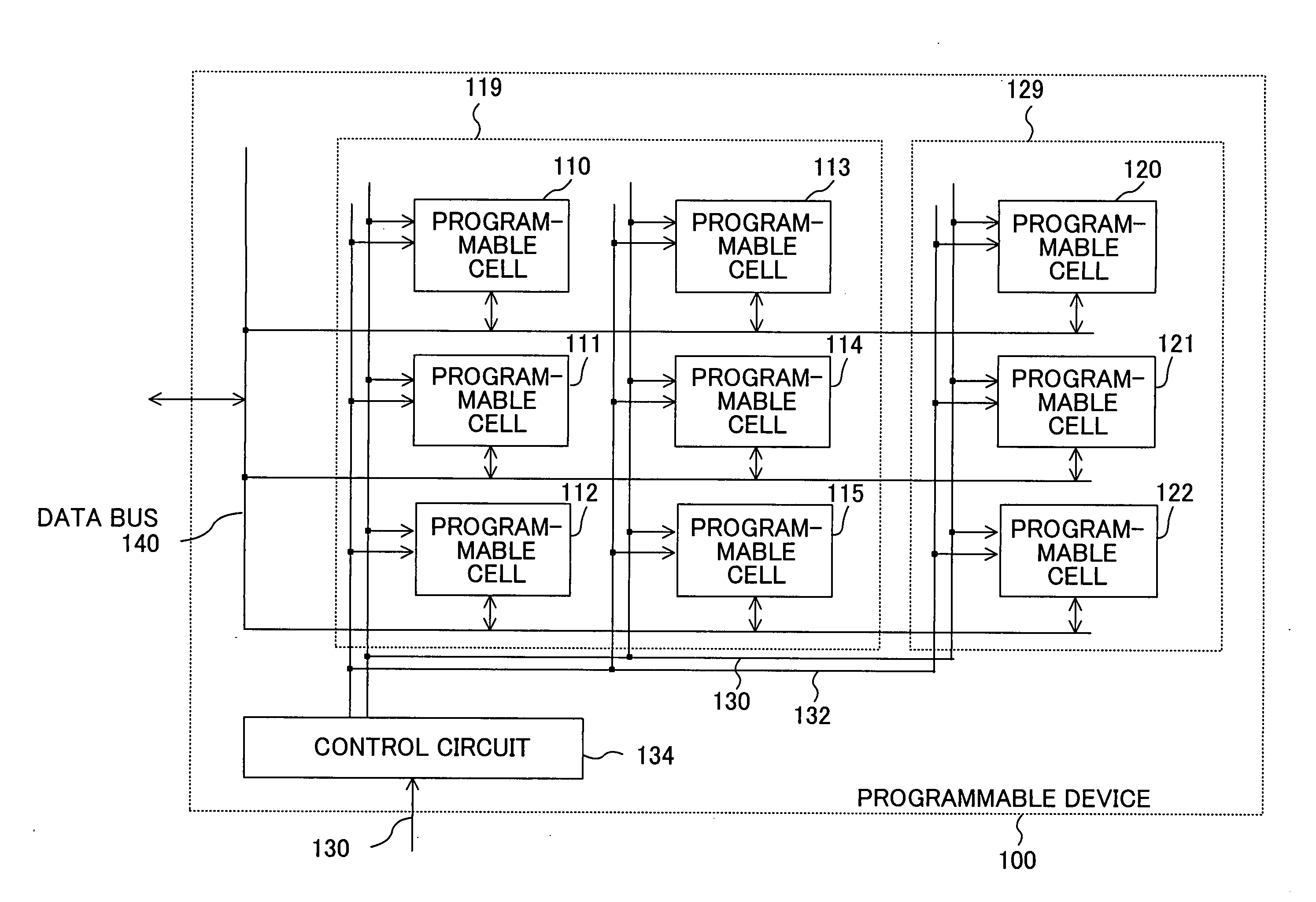
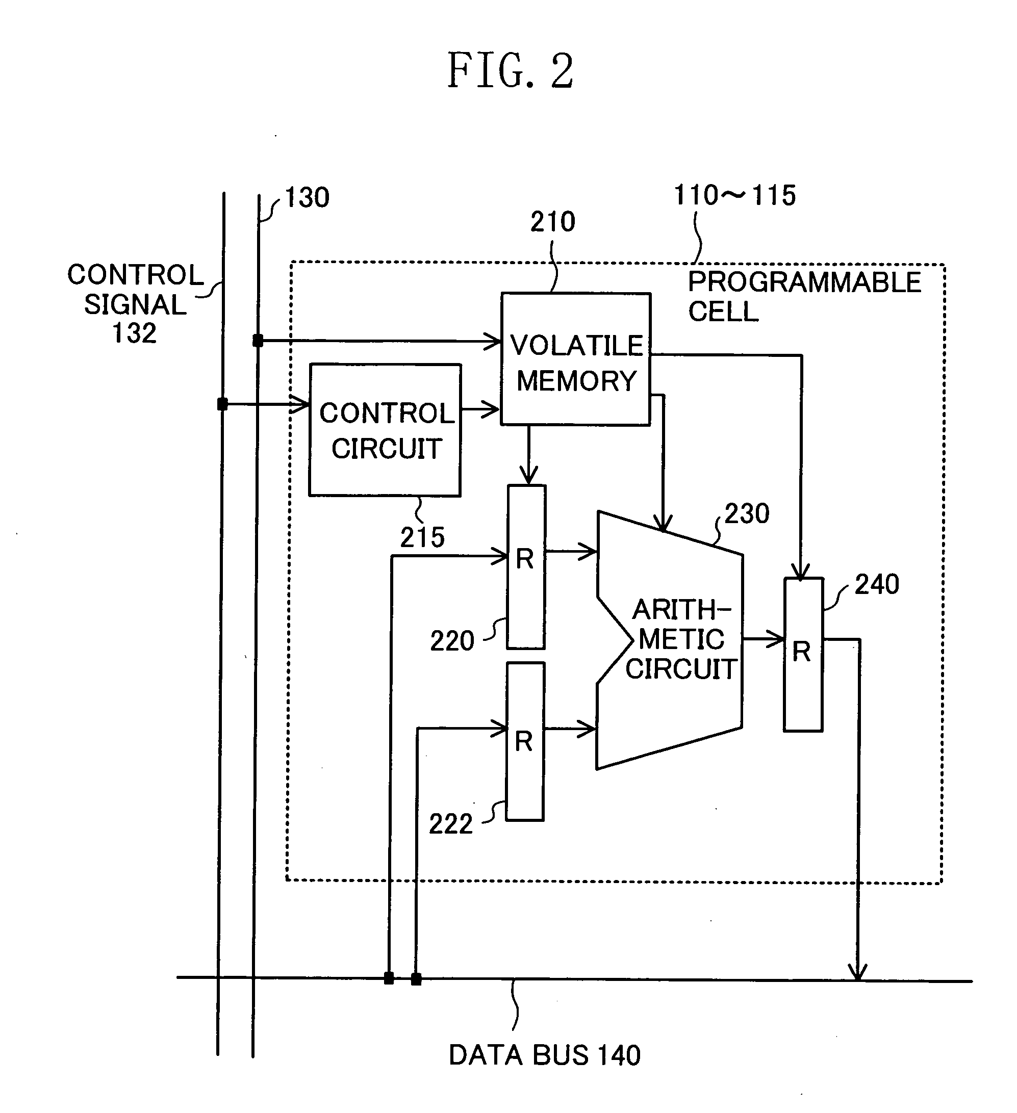
[0021]FIG. 1 illustrates the structure of a programmable device 100 according to a first embodiment. FIGS. 2 and 3 illustrate the internal structures of a plurality of programmable cells included in the programmable device 100.
[0022] The programmable device 100 shown in FIG. 1 includes a first region 119, a second region 129, a control circuit 134, and a data bus 140. The first region 119 includes first to sixth programmable cells 110 to 115 shown in FIG. 2. The second region 129 includes seventh to ninth programmable cells 120 to 122 shown in FIG. 3. The control circuit 134 receives configuration information 130 supplied from a block (not shown) and outputs the configuration information 130 and a control signal 132 indicating in which programmable cell the configuration information 130 is to be stored. The data bus 140 provides the first to ninth programmable cells 110 to 115 and 120 to 122 with data on which operations are to be performed.
[0023] The first to sixth programmable c...
second embodiment
[0031]FIG. 5 illustrates the structure of a programmable device 500 according to a second embodiment. FIGS. 6 and 7 illustrate the internal structures of a plurality of programmable cells included in the programmable device 500.
[0032] The programmable device 500 shown in FIG. 5 includes a first region 519, a second region 529, a control circuit 534, and a data bus 540. The first region 519 includes first to sixth programmable cells 510 to 515 shown in FIG. 6. The second region 529 includes seventh to ninth programmable cells 520 to 522 shown in FIG. 7. The control circuit 534 receives configuration information 530 supplied from a block (not shown) and outputs a first write signal 532, a second write signal 533, and the configuration information 530. The first write signal 532 indicates that the configuration information 530 is to be stored in the first to sixth programmable cells 510 to 515. The second write signal 533 indicates that the configuration information 530 is to be store...
third embodiment
[0041]FIG. 8 illustrates the structure of a programmable device 800 according to a third embodiment. FIG. 9 illustrates the internal structures of tenth to twelfth programmable cells 820 to 822 included in the programmable device 800.
[0042] The programmable device 800 shown in FIG. 8 differs from the programmable device 100 shown in FIG. 1 in that the programmable device 800 has, in addition to the above-described first and second regions 119 and 129, a third region 829 in which the tenth to twelfth programmable cells 820 to 822 are included, and that the tenth to twelfth programmable cells 820 to 822 shown in FIG. 9 have ROMs 910 in which information equivalent to the configuration information 130 is stored beforehand. Therefore, if process, whose operation contents do not require any changes after the shipment of the LSI having the programmable device 800 mounted thereon, is stored beforehand in the respective ROMs 910 included in the tenth to twelfth programmable cells 820 to 82...
PUM
 Abstract
Description
Claims
Application Information