Printed circuit board having shield structure of signal transmission line

a shield structure and signal transmission technology, applied in the direction of non-printed jumper connection addition, waveguide, semiconductor/solid-state device details, etc., can solve the problem that the arrangement of signal transmission lines on the opposite surface may also serve as a limiting factor, and achieve the effect of reducing the likelihood of coupling nois

Inactive Publication Date: 2006-06-08
SAMSUNG ELECTRONICS CO LTD
View PDF4 Cites 21 Cited by
  • Summary
  • Abstract
  • Description
  • Claims
  • Application Information

AI Technical Summary

Benefits of technology

[0011] An example embodiment of the present invention provides a printed circuit board for a high-speed semiconductor package with reduced likelihood of coupling noises between signal transmission lines.
[0012] Another example embodiment of the present invention provides a printed circuit board for high-speed semiconductor package with reduced likelihood of coupling noises caused by surface waves.

Problems solved by technology

In the case of through-hole vias, signal transmission line arrangements on the opposite surface may also serve as a limiting factor.

Method used


Image

  • Printed circuit board having shield structure of signal transmission line
  • Printed circuit board having shield structure of signal transmission line
  • Printed circuit board having shield structure of signal transmission line

Examples


Embodiment Construction

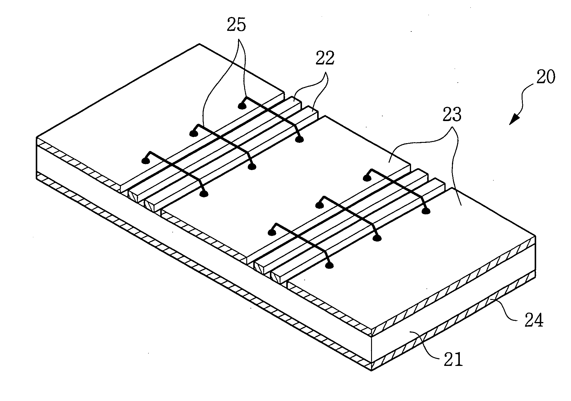
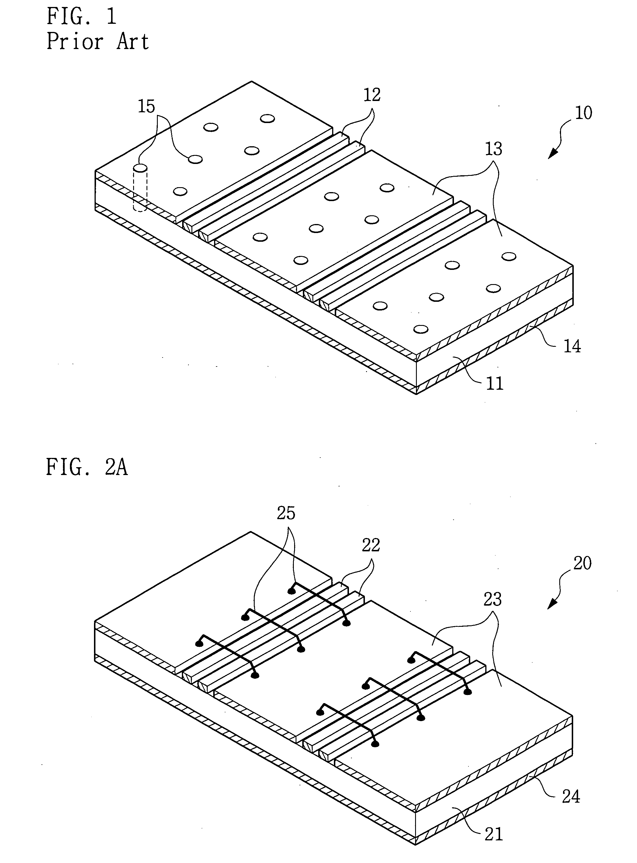
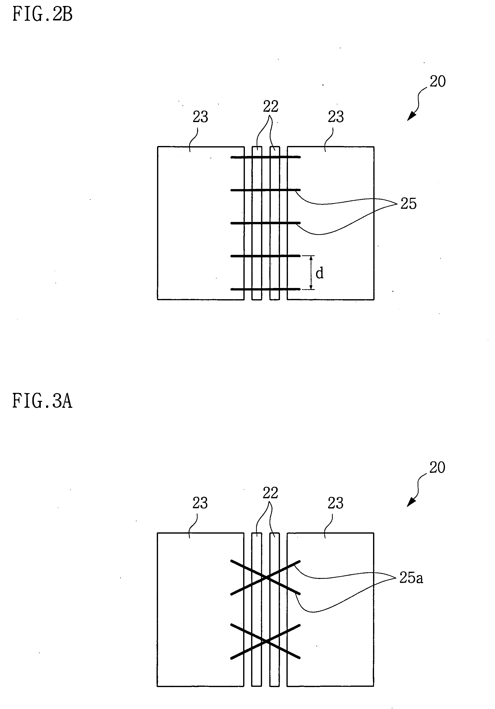
[0025] Example, non-limiting embodiments of the present invention will now be described more fully hereinafter with reference to the accompanying drawings. This invention may, however, be embodied in many different forms and should not be construed as limited to the example embodiments set forth herein. Rather, the disclosed embodiments are provided so that this disclosure will be thorough and complete, and will fully convey the scope of the invention to those skilled in the art. The principles and features of this invention may be employed in varied and numerous embodiments without departing from the scope of the invention.

[0026] It should be noted that the figures are intended to illustrate the general characteristics of methods and devices of example embodiments of this invention and support the description of such example embodiments herein. These drawings are not, however, to scale and may not precisely reflect the characteristics of any given embodiment, and should not be int...


PUM


Abstract

A printed circuit board for a high-speed semiconductor package uses bonding wires as a shield structure, e.g., to shield an open portion of signal transmission lines, and thereby reduce the likelihood of coupling noises, e.g., between signal transmission lines.

Description

CROSS REFERENCE TO RELATED APPLICATIONS [0001] This U.S. non-provisional application claims benefit of priority under 35 U.S.C. §119 of Korean Patent Application No. 2004-102368, filed on Dec. 7, 2004, the entire contents of which are incorporated herein by reference. BACKGROUND OF THE INVENTION [0002] 1. Field of the Invention [0003] The present invention relates to a printed circuit board for a high-speed semiconductor package and, more particularly, to a printed circuit board having a shield structure for high-speed signal transmission lines. [0004] 2. Description of the Related Art [0005] The advance of data transmitting / receiving techniques may incorporate semiconductor products for transmitting high-speed signals, for example of several Gbps (Gigabits per second). Generally, high-speed semiconductor products may be manufactured in a ball grid array (BGA) package type. The BGA package type may require printed circuit boards (PCBs) having a signal transmission line structure. Th...

Claims


Application Information

Patent Timeline
Patent Type & Authority Applications(United States)
IPC IPC(8): H01P3/08
CPCH01L24/45H01L24/49H01L2224/45015H01L2224/45124H01L2224/45139H01L2224/45144H01L2224/45147H01L2224/48095H01L2224/4917H01L2224/49175H01L2224/85201H01L2224/85205H01L2924/01004H01L2924/01005H01L2924/01012H01L2924/01013H01L2924/01014H01L2924/01029H01L2924/01047H01L2924/01079H01L2924/14H01L2924/20751H01L2924/20752H01L2924/20753H01L2924/20754H01L2924/20755H01L2924/3025H01P3/003H01P3/08H05K1/0219H05K3/222H05K2201/09236H05K2203/049H01L2924/00014H01L2924/01006H01L2924/01033H01L2924/00H01L2924/19107H01L24/48H01L2924/013H01L2924/00013H01L23/12H01L21/60
Inventor LEE, HEE-SEOKJANG, KYUNG-LAECHO, TAE-JECHOI, KI-WON
Owner SAMSUNG ELECTRONICS CO LTD
Why Eureka
Try Eureka