

Switching circuits
a technology of switching circuit and circuit, applied in the direction of electronic switching, pulse technique, semiconductor devices, etc., can solve the problems of large area, inducing signal distortion, and requiring large area for increasing contacts
- Summary
- Abstract
- Description
- Claims
- Application Information
AI Technical Summary
Benefits of technology
Problems solved by technology
Method used
Image

Examples
first embodiment
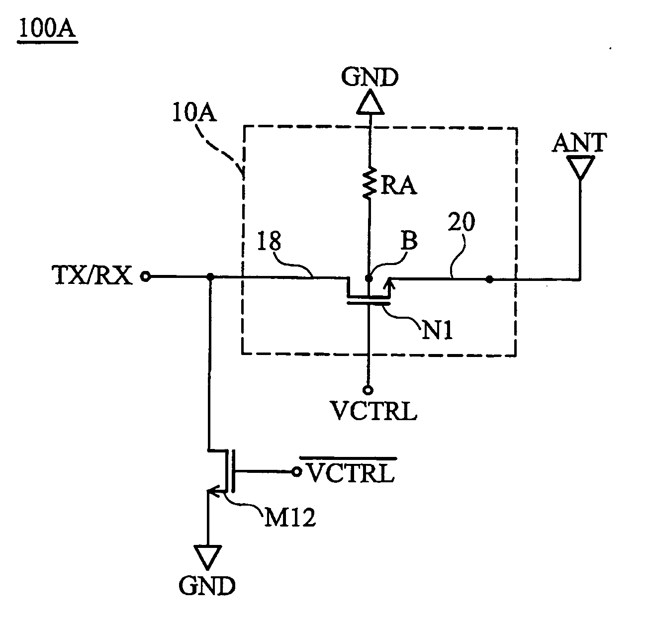
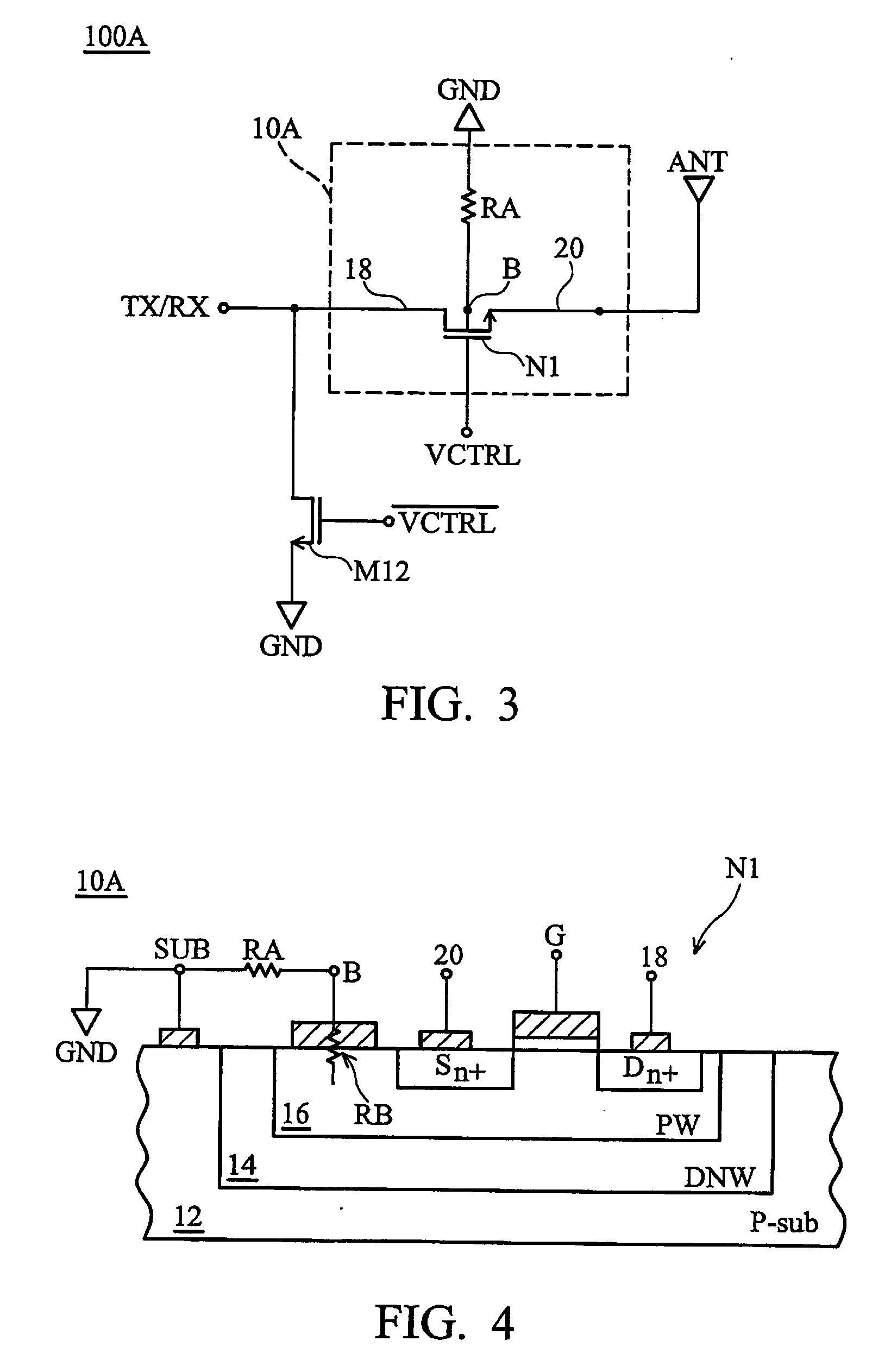
[0026]FIG. 3 shows a radio frequency (RF) switching circuit. As shown, the switching circuit 100A comprises two switching elements 10A and M12. The switching element 10A comprises a first terminal 18 coupled to an output / input terminal TX / RX, a second terminal 20 coupled to an antenna element ANT, a control terminal coupled to a control signal VCTRL and a bulk terminal B coupled to the ground voltage GND through a first external resistive element RA. The switching element M12 comprises a control terminal coupled to an inversion signal of the control signal VCTRL, a first terminal coupled to the ground voltage GND, and a second terminal coupled to the output / input terminal TX / RX. The switching element 10A is turned on, according to the control signal VCTRL, to transmit a signal received by the antenna element ANT to the output / input terminal TX / RX or a signal output from the output / input terminal TX / RX to the antenna element ANT.
[0027]FIG. 4 shows the structure of switching element 1...
second embodiment
[0031]FIG. 7 shows a single-pole double-throw (SPDW) RF switching circuit. As shown, the switching circuit 100B comprises switching elements N1a, N1b, M14 and M16, in which the switching elements M14 and M16 are normal NMOS transistors, and the switching elements N1a and N1b are both similar to the switching element 10A shown in FIG. 4.
[0032] The switching element N1a comprises a drain terminal coupled to an output / input terminal TX1 / RX1, a source terminal coupled to an antenna element ANT, a control terminal coupled to a control signal VCTRL through a resistor R1 and a bulk terminal coupled to the ground voltage GND through a first external resistive element RA1. The switching element N1b comprises a drain terminal coupled to an output / input terminal TX2 / RX2, a source terminal coupled to an antenna element ANT, a control terminal coupled to an inversion signal {overscore (VCTRL)} of the control signal VCTRL through a resistor R2 and a bulk terminal coupled to the ground voltage GND...
fourth embodiment
[0039]FIG. 11 shows another single pole dual throw (SPDW) RF switching circuit. As shown, the switching circuit 100D comprises switching elements N1c, N1d, M14 and M16, in which the switching elements M14 and M16 are normal NMOS transistors, and the switching elements N1c and N1d both are similar to the switching element 10D shown in FIG. 10.
[0040] The switching element N1c comprises a drain terminal coupled to an output / input terminal TX1 / RX1, a source terminal coupled to an antenna element ANT, a control terminal coupled to a control signal VCTRL and a bulk terminal coupled to the source terminal thereof through a first external resistive element RA1. The switching element N1d comprises a drain terminal coupled to an output / input terminal TX2 / RX2, a source terminal coupled to an antenna element ANT, a control terminal coupled to an inversion signal {overscore (VCTRL)} of the control signal VCTRL and a bulk terminal coupled to the source terminal thereof through a second external r...
PUM
 Abstract
Description
Claims
Application Information