
Substrate processing apparatus

a processing apparatus and substrate technology, applied in the field of substrate processing apparatus, can solve the problems of requiring about two minutes, affecting the uniformity of the line width of the pattern, and no particular consideration has been given to controlling the time interval. , to achieve the effect of improving the line width uniformity of the pattern

Inactive Publication Date: 2006-06-08
DAINIPPON SCREEN MTG CO LTD
View PDF4 Cites 10 Cited by
  • Summary
  • Abstract
  • Description
  • Claims
  • Application Information

AI Technical Summary

Benefits of technology

[0011] According to the present invention, the substrate processing apparatus comprises: a coating processing part for performing a resist coating process on a substrate; a development processing part for performing a development process on an exposed substrate; an interface part for receiving a substrate with a resist film formed thereon by the resist coating process from the coating processing part to transfer the substrate to an exposure apparatus, and for receiving an exposed substrate from the exposure apparatus to transfer the exposed substrate to the development processing part; an indexer part for transferring an unprocessed substrate received from the outside of the substrate processing apparatus outwardly therefrom to the coating processing part, and for transporting a processed substrate received from the development processing part to the outside of the substrate processing apparatus; a transport part for transporting a substrate between the coating processing part, the development processing part, the interface part and the indexer part; and a control part for controlling the transport part to provide a constant time interval between the completion of the resist coating process of substrates in the coating processing part and the execution of an exposure process of the substrates in the exposure apparatus.
[0013] It is therefore an object of the present invention to provide a substrate processing apparatus capable of improving the line width uniformity of a pattern.

Problems solved by technology

Unfortunately, some variations in line width occur even if the time interval between the end of the exposure process and the start of the post-exposure bake process is made constant.
However, no particular consideration has conventionally been given to controlling this time interval.
In particular, the replacement of a current exposure pattern for printing with another involves a reticle change in the exposure apparatus, which in turn requires about two minutes.

Method used


Image

  • Substrate processing apparatus
  • Substrate processing apparatus
  • Substrate processing apparatus

Examples


Embodiment Construction

[0023] A preferred embodiment according to the present invention will now be described in detail with reference to the drawings.

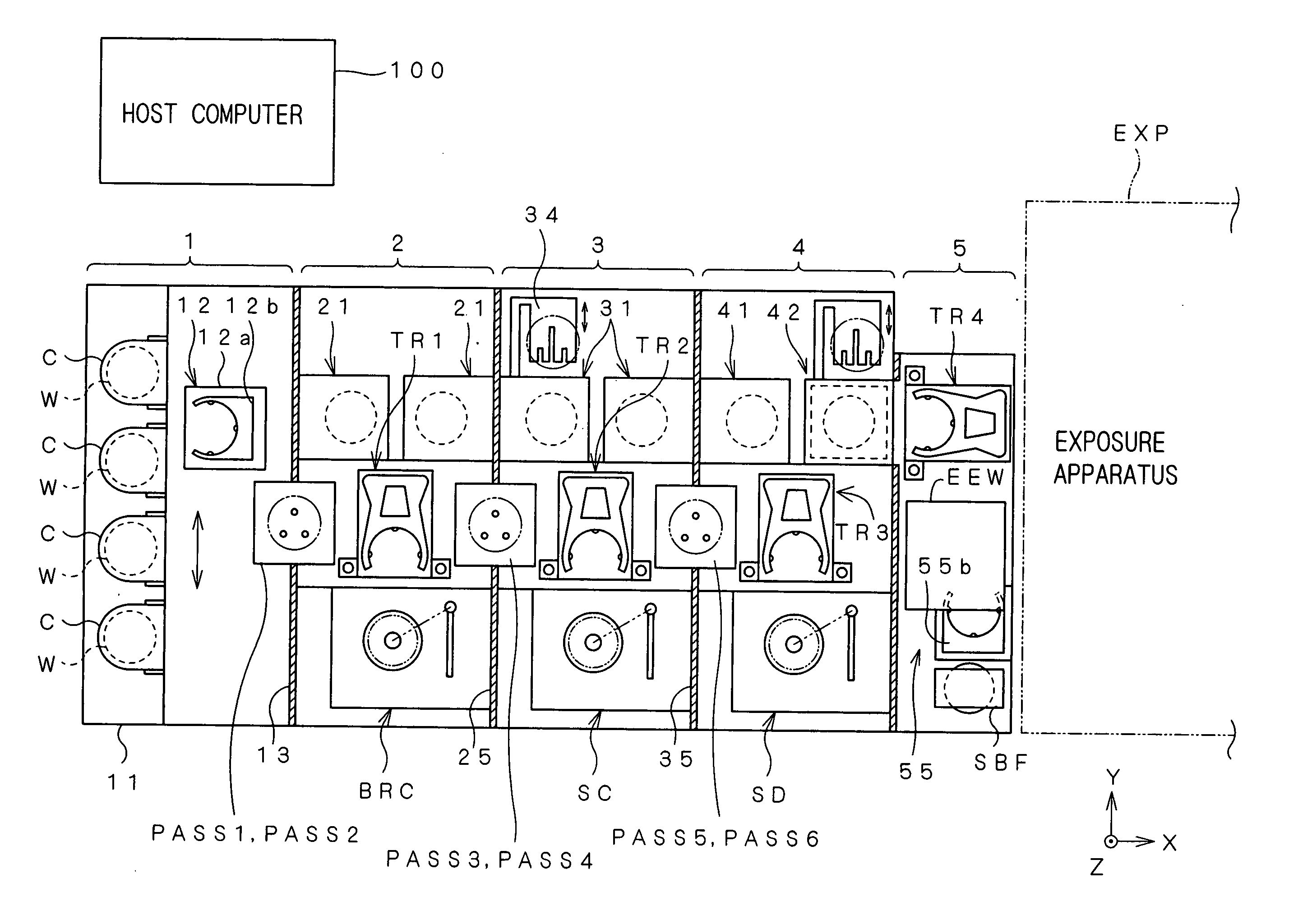
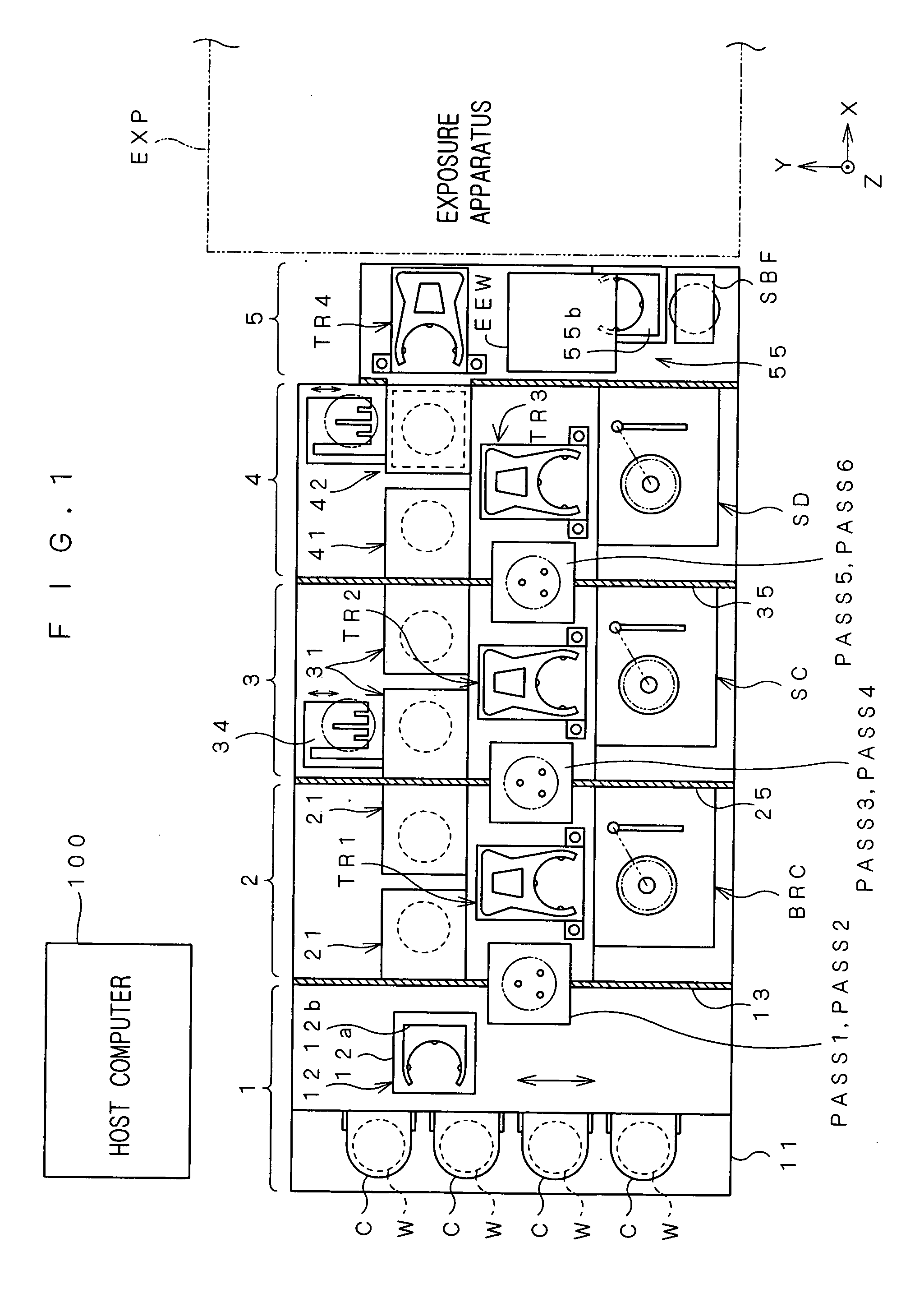
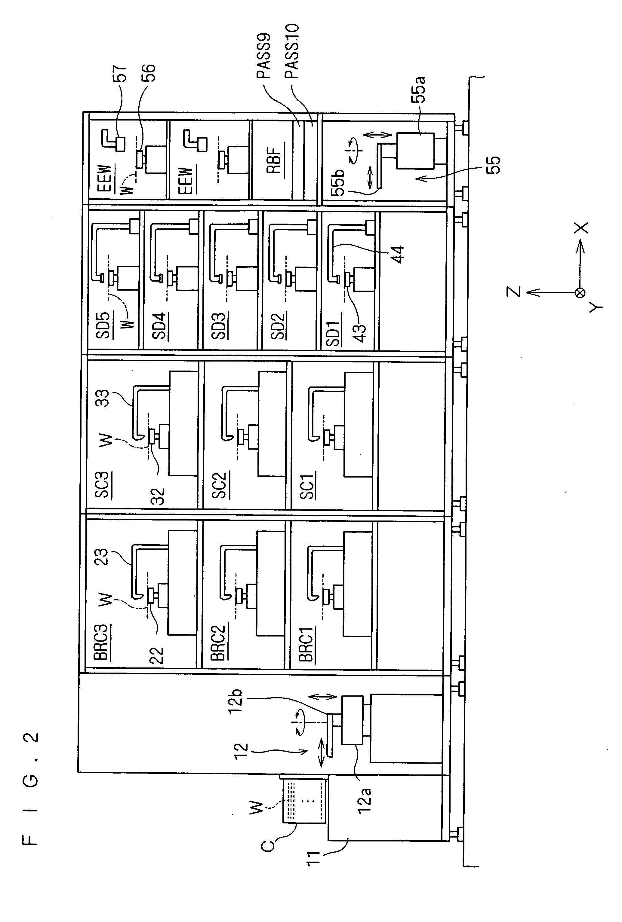
[0024]FIG. 1 is a plan view of a substrate processing apparatus according to the preferred embodiment of the present invention. FIG. 2 is a front view of a liquid processing part in the substrate processing apparatus. FIG. 3 is a front view of a thermal processing part in the substrate processing apparatus. FIG. 4 is a view showing a construction around substrate rest parts in the substrate processing apparatus. An XYZ rectangular coordinate system in which an XY plane is defined as the horizontal plane and a Z axis is defined to extend in the vertical direction is additionally shown in FIGS. 1 through 4 for purposes of clarifying the directional relationship therebetween.

[0025] The substrate processing apparatus according to the preferred embodiment is an apparatus for forming an anti-reflective film and a photoresist film on substrates such as semicondu...


PUM


Abstract

When a first substrate transferred outwardly from an indexer cell is the last substrate prior to reticle change in an exposure apparatus, the outward transfer of a second substrate to be processed subsequently to the first substrate from the indexer cell is temporarily stopped. After a lapse of time corresponding to reticle replacement time, the outward substrate transfer is restarted, and the second substrate is transferred outwardly from the indexer cell. For the exposure apparatus, the second substrate subjected to a resist coating process is received at the instant when the reticle replacement is completed after the completion of the exposure process of the first substrate. This provides a constant time interval between the completion of the resist coating process of substrates and the execution of the exposure process thereof without the decrease in processing efficiency. As a result, a uniform processing history for the substrates is achieved to further improve the line width uniformity of a pattern.

Description

BACKGROUND OF THE INVENTION [0001] 1. Field of the Invention [0002] The present invention relates to a substrate processing apparatus for transporting a substrate, such as a semiconductor substrate, a glass substrate for a liquid crystal display device, a glass substrate for a photomask, a substrate for an optical disk and the like, with a resist film formed thereon by coating the substrate with a resist into an exposure apparatus, and for performing a development process on an exposed substrate received from the exposure apparatus. [0003] 2. Description of the Background Art [0004] As is well known, semiconductor and liquid crystal display products and the like are fabricated by performing a series of processes including cleaning, resist coating, exposure, development, etching, interlayer insulation film formation, heat treatment, dicing and the like on the above-mentioned substrate. An apparatus which performs a resist coating process on a substrate to transfer the substrate to an...

Claims


Application Information

Patent Timeline
Patent Type & Authority Applications(United States)
IPC IPC(8): G03D5/00
CPCG03F7/168G03F7/2006H01L21/67225H01L21/67748
Inventor HAMADA, TETSUYA
Owner DAINIPPON SCREEN MTG CO LTD
Learn More