Conductive ink, organic semiconductor transistor using the conductive ink, and method of fabricating the transistor

Inactive Publication Date: 2006-06-15
ELECTRONICS & TELECOMM RES INST
View PDF3 Cites 49 Cited by
  • Summary
  • Abstract
  • Description
  • Claims
  • Application Information

AI Technical Summary

Benefits of technology

[0008] The present invention is directed to a conductive ink, which is used to form electrodes using a direct printing process during the fabrication of an organic thin-film transistor (OTFT). Above all, even if the conductive ink is formed on a

Problems solved by technology

However, the direct printing process re

Method used


Image

  • Conductive ink, organic semiconductor transistor using the conductive ink, and method of fabricating the transistor
  • Conductive ink, organic semiconductor transistor using the conductive ink, and method of fabricating the transistor

Examples


Embodiment Construction

[0015] The present invention will now be described more fully hereinafter with reference to the accompanying drawings, in which preferred embodiments of the invention are shown. This invention may, however, be embodied in different forms and should not be construed as limited to the embodiments set forth herein. Rather, these embodiments are provided so that this disclosure is thorough and complete and fully conveys the scope of the invention to those skilled in the art.

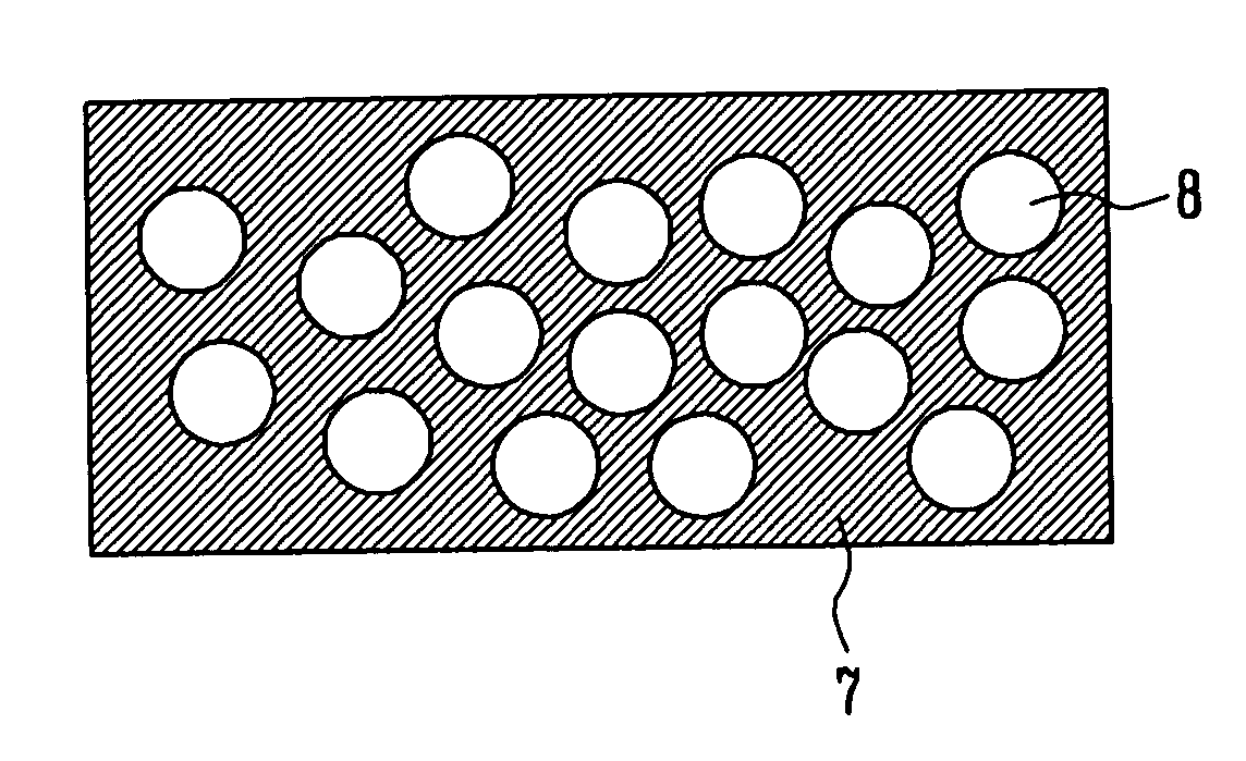
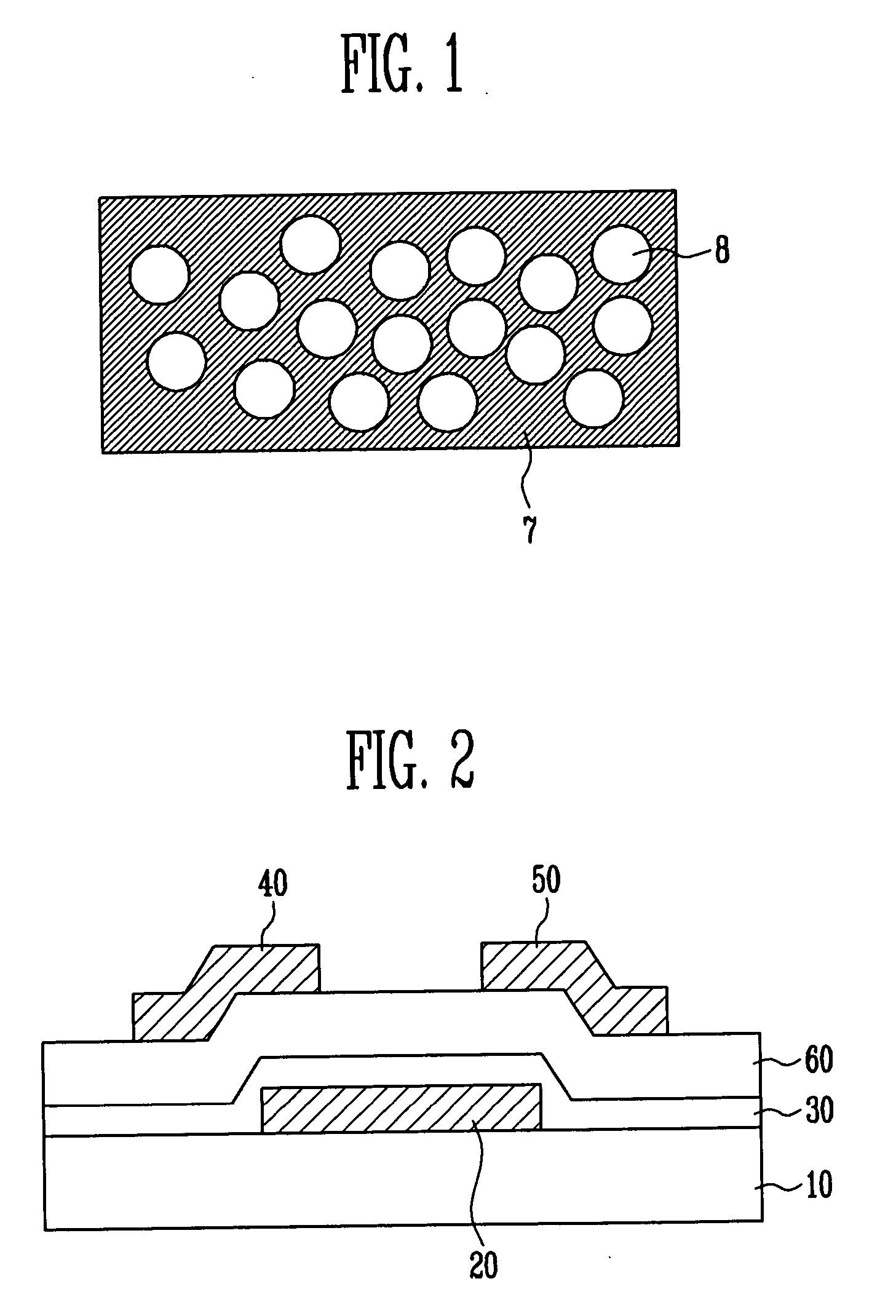
[0016]FIG. 1 is a conceptual diagram of a conductive ink according to an exemplary embodiment of the present invention.

[0017] Referring to FIG. 1, the conductive ink according to the present invention includes a conductive polymer 7 and metal nanoparticles 8. The conductive polymer 7 is highly flexible, has a large work function, and may be used as a conductive ink for a direct printing process. However, the conductive polymer 7 is even less conductive than a metal thin layer. Also, the metal nanoparticles 8 includ...


PUM

PropertyMeasurementUnit
Fractionaaaaaaaaaa
Nanoscale particle sizeaaaaaaaaaa
Concentrationaaaaaaaaaa

Abstract

Provided are a conductive ink, organic semiconductor transistor using the conductive ink, and method of fabricating the transistor. The conductive ink is used to form electrodes on an organic semiconductor while minimizing the damage of the organic semiconductor. The conductive ink is formed by mixing metal nanoparticles with a conductive polymer and used as an electrode material during the fabrication of the organic semiconductor transistor using a direct printing process. By using the conductive ink as the electrode material, the production cost of the organic semiconductor transistor can be greatly reduced.

Description

CROSS-REFERENCE TO RELATED APPLICATION [0001] This application claims priority to and the benefit of Korean Patent Application No. 2004-103688, filed Dec. 9, 2004, the disclosure of which is incorporated herein by reference in its entirety. BACKGROUND [0002] 1. Field of the Invention [0003] The present invention relates to a conductive ink used for electrodes of an organic semiconductor thin-film transistor (OTFT) and, more specifically, to a conductive ink suitable for a direct printing process, OTFT using the conductive ink, and method of fabricating the OTFT. [0004] 2. Discussion of Related Art [0005] Most generally, an organic field effect transistor (OFET) fabricated on an insulating substrate using an organic semiconductor thin layer is defined as an organic semiconductor thin-film transistor (OTFT). Like a field effect transistor (FET), the OTFT includes three terminals of a gate, a source, and a drain and is mainly used as a switching device. The OTFT may be applied to a sen...

Claims


Application Information

Patent Timeline
IPC IPC(8): H01L29/08
CPCH01L51/0022H01L51/0037H01L51/0541H01L51/0545H01L51/105H10K71/611H10K85/1135H10K10/466H10K10/464H10K10/84H01L21/18B82Y30/00H10K99/00
Inventor KIM, SEONG HYUNZYUNG, TAE HYOUNGLEE, JUNG HUN
Owner ELECTRONICS & TELECOMM RES INST
Why Eureka
Try Eureka