Methods of reducing floating body effect

a floating body effect and memory cell technology, applied in the field of integrated circuit fabrication, can solve problems such as memory failure through cell capacitor discharge, and achieve the effect of reducing the floating body effect in the memory cell

Active Publication Date: 2006-06-15
MICRON TECH INC
View PDF7 Cites 39 Cited by
  • Summary
  • Abstract
  • Description
  • Claims
  • Application Information

AI Technical Summary

Problems solved by technology

This current can cause memory failures through cell capacitor discharge.

Method used


Image

  • Methods of reducing floating body effect
  • Methods of reducing floating body effect
  • Methods of reducing floating body effect

Examples


Embodiment Construction

[0030] In the context of this document, the term “semiconductor substrate” is defined to mean any construction comprising semiconductor materials, including, but not limited to, bulk semiconductor materials such as a semiconductor wafer (either alone or in assemblies comprising other materials thereon), and semiconductor material layers (either alone or in assemblies comprising other materials). The term “substrate” refers to any supporting substrate, including, but not limited to, the semiconductor substrates described above. Also in the context of this document, the term “layer” encompasses both the singular and the plural unless otherwise indicated.

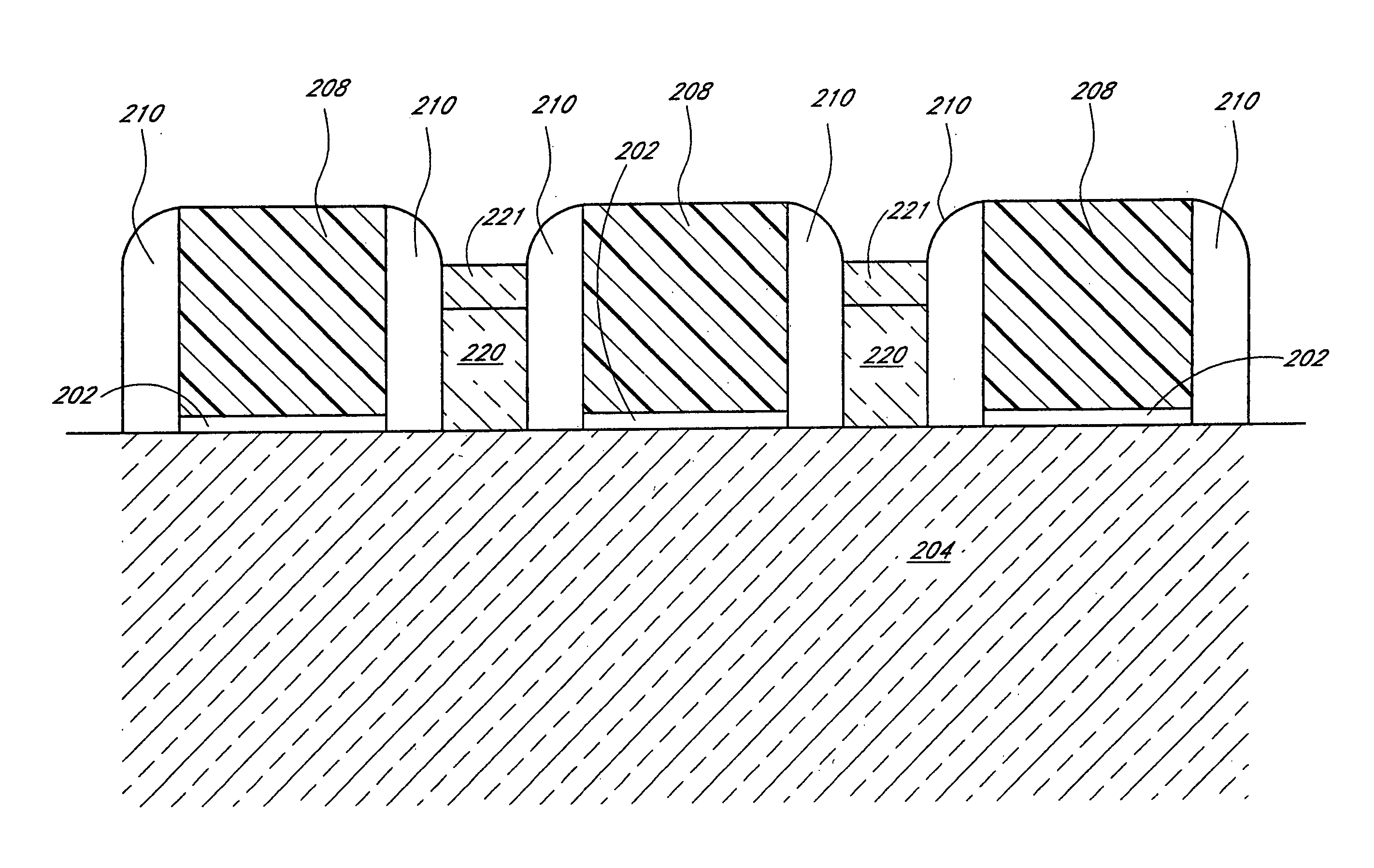
[0031] In small (e.g. 4 F2) memory cell designs, a vertical transistor can be used. These transistors typically use silicon pillars to form at least a portion of the active region. Silicon pillars can be formed using multiple masks and providing a spacer lining sidewalls of small windows before selectively growing epitaxial silicon wi...


PUM


Abstract

Methods of reducing the floating body effect in vertical transistors are disclosed. The floating body effect occurs when an active region in a pillar is cut off from the substrate by a depletion region and the accompanying electrostatic potential created. In a preferred embodiment, a word line is recessed into the substrate to tie the upper active region to the substrate. The resulting memory cells are preferably used in dynamic random access memory (DRAM) devices.

Description

BACKGROUND OF THE INVENTION [0001] 1. Field of the Invention [0002] The present invention relates to the field of integrated circuit fabrication, specifically to the formation of transistors. [0003] 2. Description of the Related Art [0004] Since the introduction of the digital computer, electronic storage devices have been a vital resource for the retention of data. Conventional semiconductor electronic storage devices, such as Dynamic Random Access Memory (DRAM), typically incorporate capacitor and transistor structures in which the capacitors temporarily store data based on the charged state of the capacitor structure. In general, this type of semiconductor Random Access Memory (RAM) often requires densely packed capacitor structures that are easily accessible for electrical interconnection. [0005] In order to increase efficiency of memory devices, there is an effort to create smaller memory cells. DRAM memory cells can shrink by decreasing the minimum feature size (F) through new...

Claims


Application Information

Patent Timeline
Patent Type & Authority Applications(United States)
IPC IPC(8): H01L29/00
CPCH01L27/0218H01L27/10823H01L27/10861H01L27/10876H01L27/10891H10B12/34H10B12/038H10B12/053H10B12/488
Inventor HALLER, GORDON A.
Owner MICRON TECH INC
Why Eureka
Try Eureka