Heterojunction photovoltaic cell

a photovoltaic cell and heterojunction technology, applied in the field of solar photovoltaic cells, can solve the problems of high manufacturing cost, complex fabrication process for junctions of dissimilar materials, and poor mobility of such materials

Inactive Publication Date: 2006-06-22
PALO ALTO RES CENT INC
View PDF10 Cites 74 Cited by
  • Summary
  • Abstract
  • Description
  • Claims
  • Application Information

AI Technical Summary

Problems solved by technology

The mobilities of such materials are often poor.
The fabrication process for junctions of dissimilar materials is usually complex, and the manufacturing cost is high.
Moreover, these cells are problematic in that there is mixing of the semiconductors at the junctions of the cells.

Method used


Image

  • Heterojunction photovoltaic cell
  • Heterojunction photovoltaic cell
  • Heterojunction photovoltaic cell

Examples


example 1

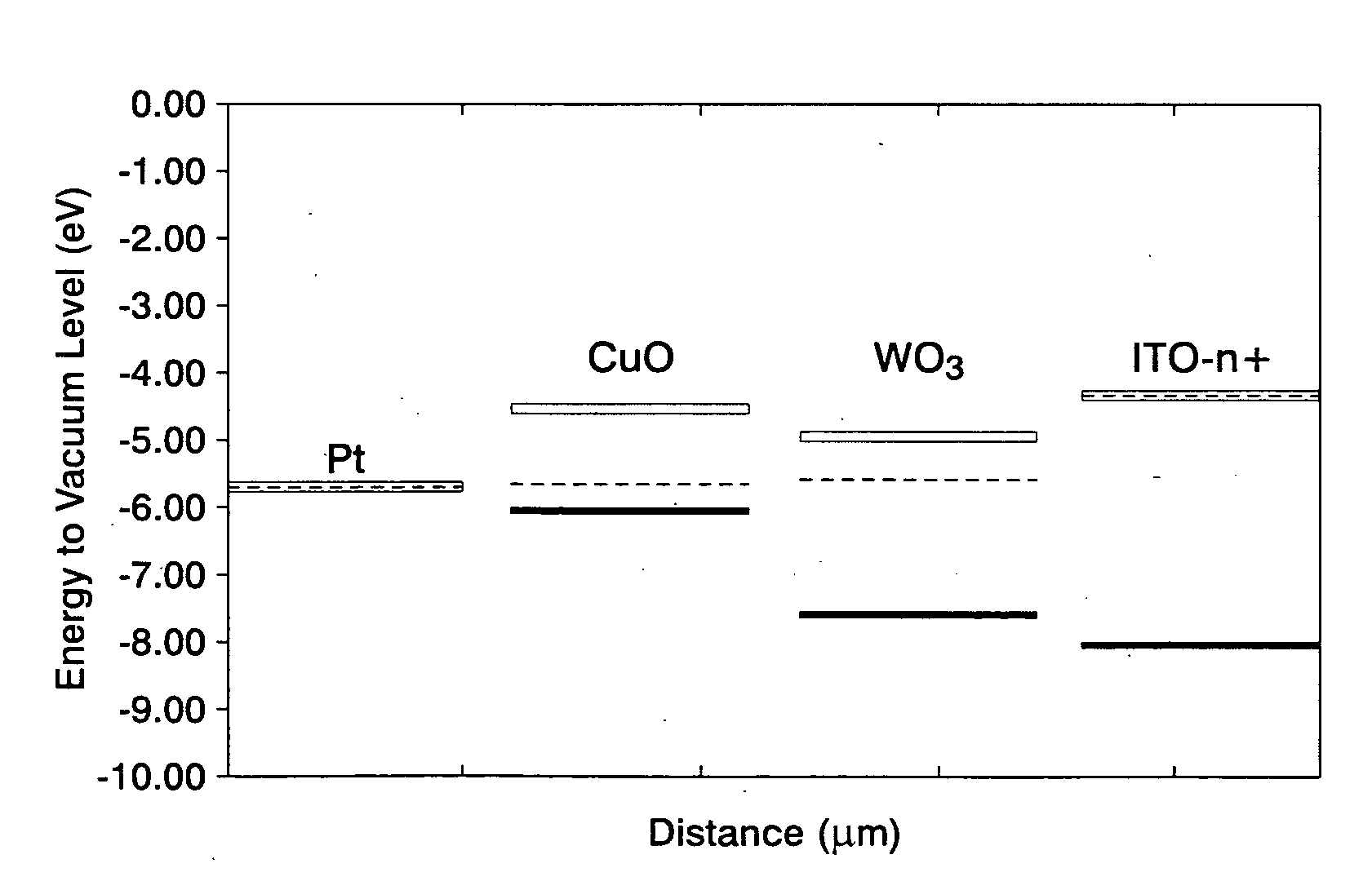
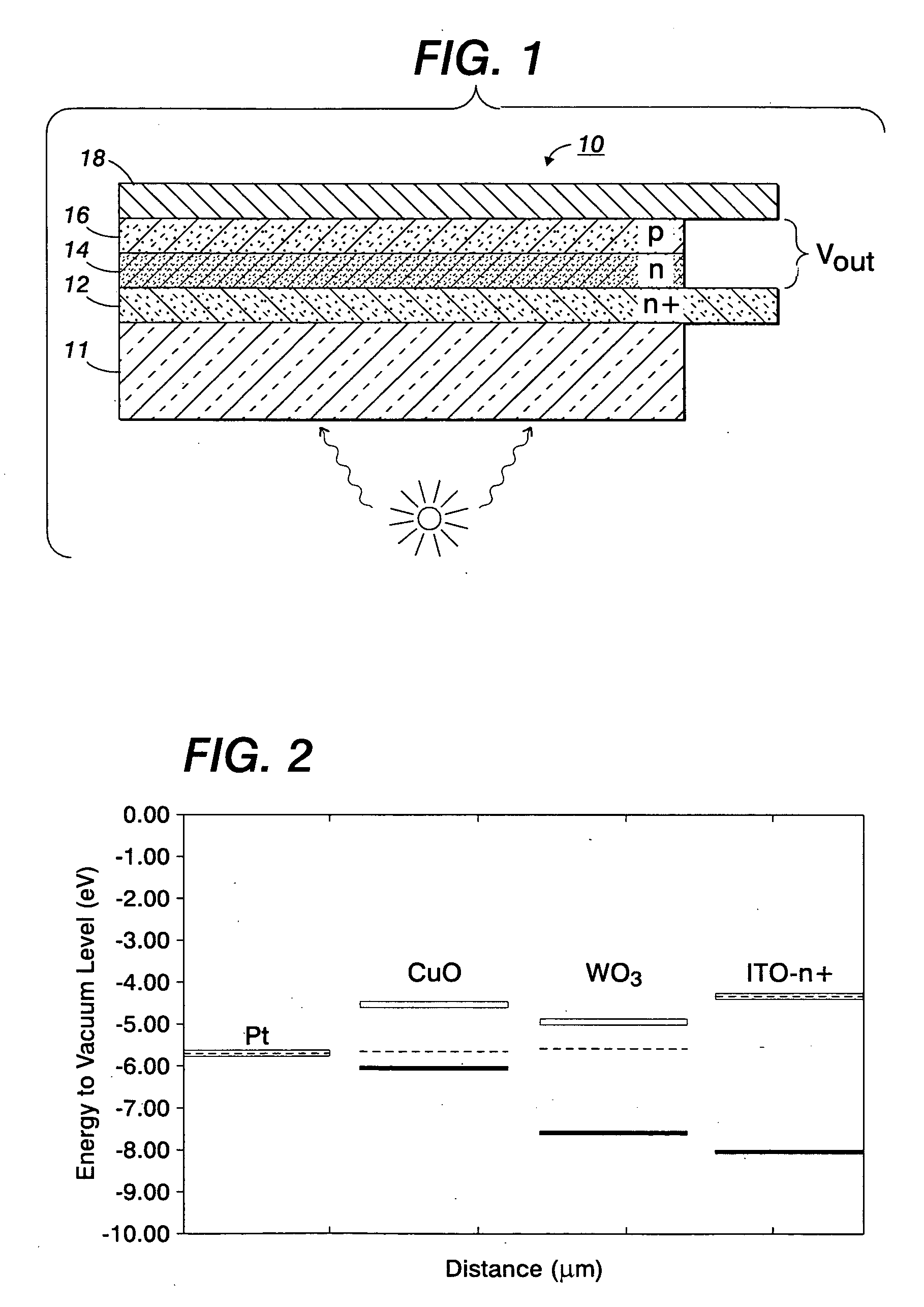
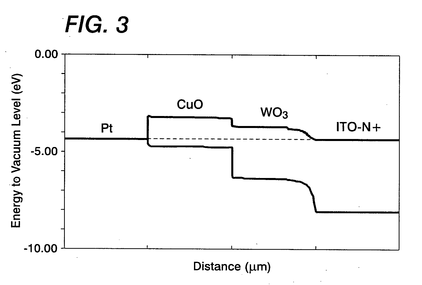
[0078] A layer of ITO was sputter deposited on a glass substrate in a manner known by one of ordinary skill in the art. A layer of tungsten of approximately 40 nm in thickness was sputter deposited on the ITO. A 40 nm layer of copper was then sputter deposited on the tungsten layer without breaking vacuum. Vacuum was then broken. The W—Cu metal stack was heated on a hot plate at 500° C. for 15 minutes to create a WO3 / CuO heterojunction.

[0079] The resultant photovoltaic device exhibited an open circuit photovoltage of approximately 0.3 volts and a closed circuit current of approximately 1.8 mA / cm2.

[0080] Including the substrate, the photovoltaic cell 10, 20 in FIGS. 1 and 5 generally has a thickness of from about 0.5 mm to about 2.0 mm.

[0081] To avoid reflection losses, the bottom side of the photovoltaic cell 10, 20, in FIGS. 1 and 5 can be provided with an antireflection coating having one, two, or more layers.

[0082] To increase the light yield, the reverse side of the photovol...


PUM


Abstract

In accordance with one aspect of the present disclosure, a solar photovoltaic device is disclosed. The semiconductor material of the solar photovoltaic device is a heterostructure of two different binary compounds of a pair of immiscible metals. The two different binary compounds have a conduction band edge offset of greater than about 0.4 eV. The binary compound acting as the optical absorbing material of the solar photovoltaic device has a bandgap of about 1.0 eV to about 1.8 eV.

Description

BACKGROUND [0001] The present disclosure relates to semiconductor devices, and more particularly, to solar photovoltaic cells. [0002] A photovoltaic cell is a component in which light is converted directly into electric energy. [0003] A heterojunction photovoltaic cell is one in which two dissimilar materials are used to generate the bias field and induce charge separation between generated electrons and holes. [0004] A heterojunction photovoltaic cell comprises at least one light-absorbing layer and a charge transport layer, as well as two electrodes. If the converted light is sunlight, the photovoltaic cell is a solar cell. [0005] For solar photovoltaic cells, one would ideally want to use low-cost, non-toxic and abundant source materials and process these materials at low temperature on inexpensive substrates. The mobilities of such materials are often poor. For example, copper oxide (CuO) has a nearly ideal band gap (1.6 eV) for a solar photovoltaic device, but has a low mobilit...

Claims


Application Information

Patent Timeline
Patent Type & Authority Applications(United States)
IPC IPC(8): H01L31/00
CPCH01L31/072H01L31/186Y02E10/50Y02P70/50
Inventor HANTSCHEL, THOMASLITTAU, KARL A.ELROD, SCOTT A.
Owner PALO ALTO RES CENT INC
Why Eureka
Try Eureka