

Organic electronic devices having two dimensional series interconnections
- Summary
- Abstract
- Description
- Claims
- Application Information
AI Technical Summary
Benefits of technology
Problems solved by technology
Method used
Image

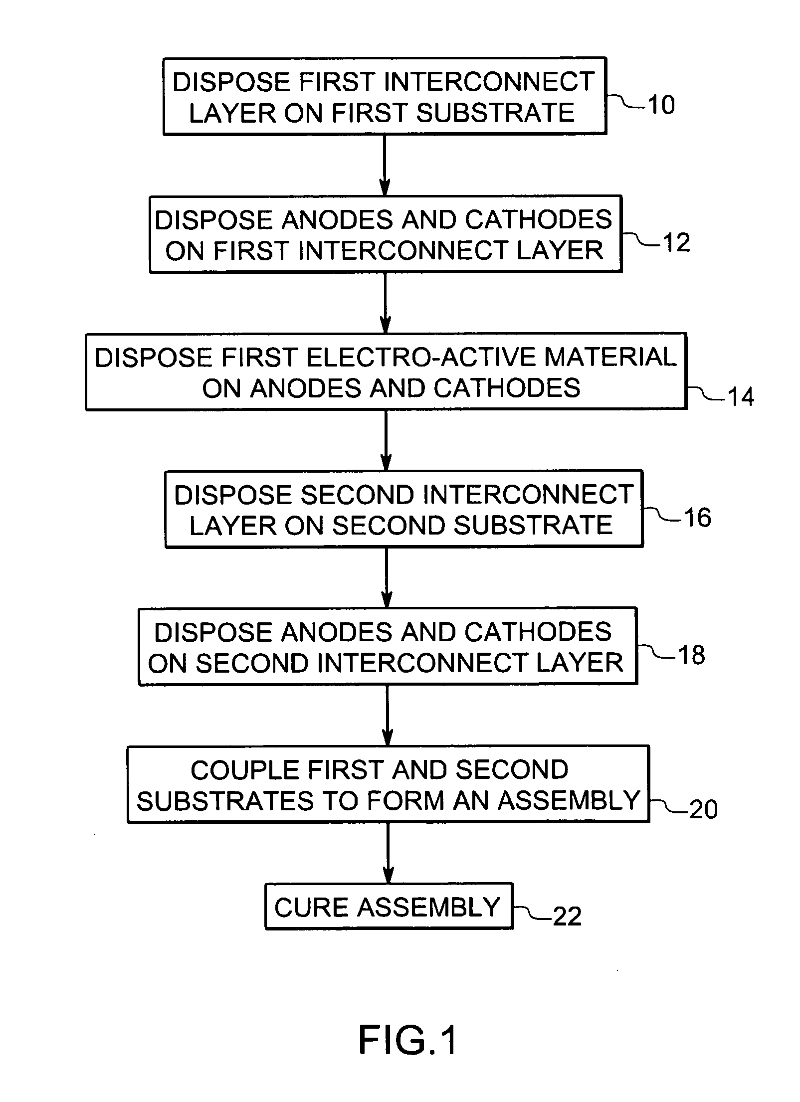
Examples
exemplary embodiment 24
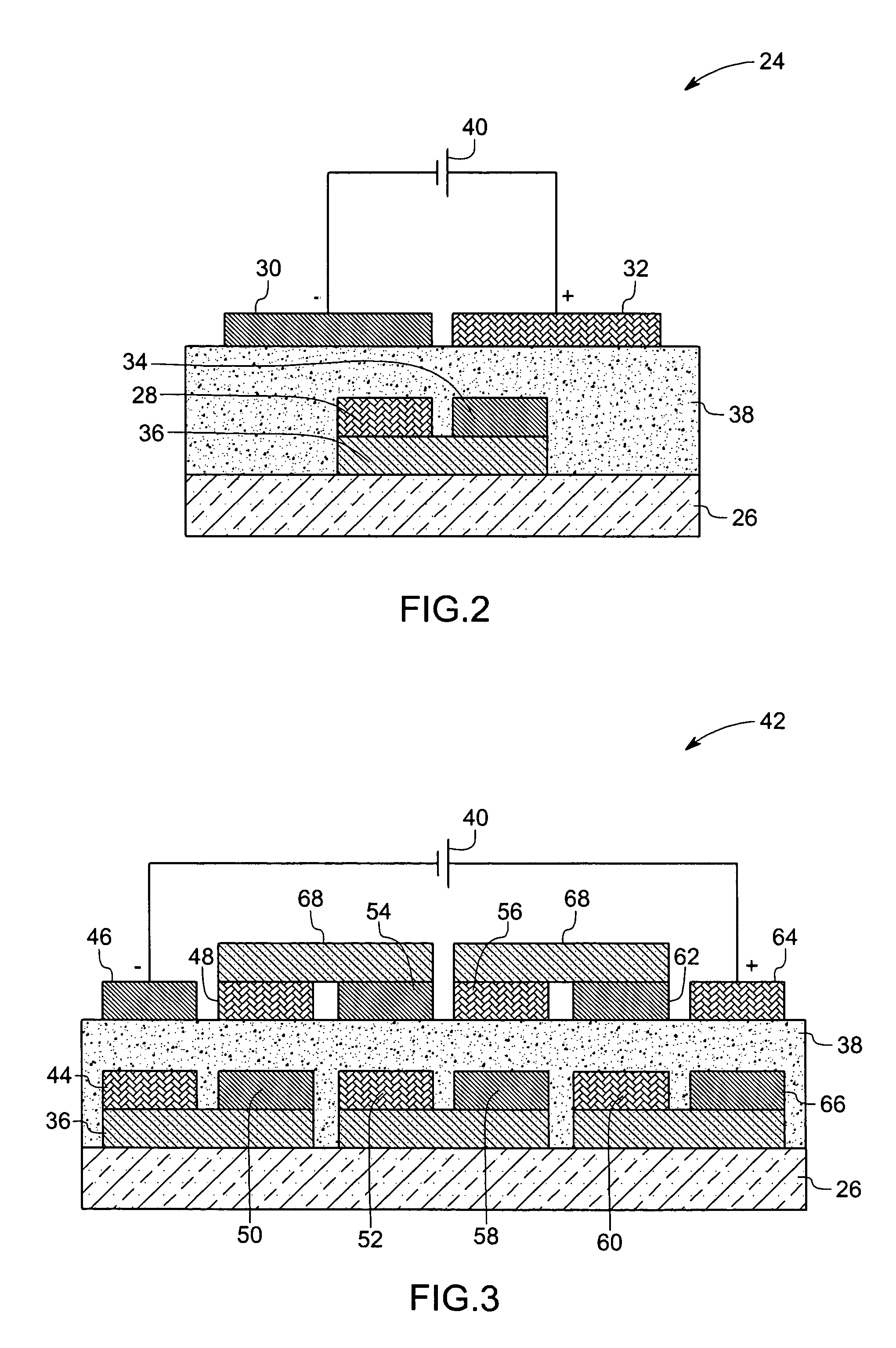
[0037] Turning to FIG. 2, a cross-sectional side view of a first exemplary embodiment 24 of a device is illustrated. In a presently contemplated configuration, the electronic device 24 is illustrated diagrammatically as including a substrate 26. According to one embodiment, the substrate 26 may include a flexible substrate, as previously described. Alternatively, the substrate 26 may include a non-flexible substrate, such as silicon, glass, or a flexible material, such as polyimide, although other types of materials with similar properties may be used.
[0038] In the illustrated embodiment, the device 24 is depicted as having first and second organic electronic devices. The first organic electronic device may include a first electrode 28 and a second electrode 30. In addition, the second organic electronic device may include a first electrode 32 and a second electrode 34. In a presently contemplated configuration, the first electrode 28 of the first organic electronic device is an ano...
exemplary embodiment 90
[0054]FIG. 6 illustrates an exemplary embodiment 90 of a device. The illustrated embodiment includes six organic electronic devices that are disposed adjacent to each other and are coupled in series. A first organic electronic device of the electronic device 90 may include an anode 92 and a cathode 94, and a second organic electronic device may include an anode 96 and a cathode 98. Similarly, the device 90 includes a third organic electronic device having an anode 100 and a cathode 102 and a fourth organic electronic device having an anode 104 and a cathode 106. Furthermore, the device 90 includes a fifth organic electronic device having an anode 108 and a cathode 110 and a sixth organic electronic device having an anode 112 and a cathode 114.
[0055] The anode 92 of the first organic electronic device may be electrically coupled in series with the cathode 98 of the second organic electronic device. In a similar fashion, the anode 100 of the third organic electronic device may be elec...
exemplary embodiment 116
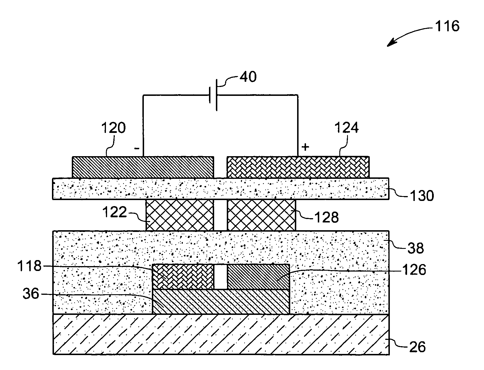
[0057]FIG. 7 illustrates an exemplary embodiment 116 of a device. In this embodiment, each of the plurality of organic electronic devices in the device 116 includes an anode, a cathode and an intermediate electrode disposed between the anode and cathode. For example, a first organic electronic device includes an anode 118, a cathode 120 and an intermediate electrode, such as a first intermediate electrode 122, disposed between the anode 118 and cathode 120 of the first organic electronic device. Similarly, a second organic electronic device includes an anode 124, a cathode 126 and an intermediate electrode, such as a second intermediate electrode 128, disposed between the anode 124 and cathode 126 of the second organic electronic device. In one embodiment, the first and second intermediate electrodes 122, 128, may include ITO. Alternatively, the first and second intermediate electrodes 122, 128, may include transparent carbon nanotubes.
[0058] The first and second organic electronic ...
PUM
 Abstract
Description
Claims
Application Information