Test method, control circuit and system for reduced time combined write window and retention testing

a control circuit and write window technology, applied in the field of reducing time, can solve problems such as loss of retention time, defects may occur, and further complicated wordline/bitline architectures

Inactive Publication Date: 2006-06-22
INFINEON TECH AG
View PDF10 Cites 73 Cited by
  • Summary
  • Abstract
  • Description
  • Claims
  • Application Information

AI Technical Summary

Benefits of technology

[0006] Briefly, a method, test mode circuit and system for a combined write window and retention test for a memory device is provided that is faster than techniques heretofore known. The combined write window and retention test procedure involves controlling time intervals during which wordlines are activated and deactivated and bitlines are grounded or connected to a bitline high voltage such that the wordlines are activated while bitlines are either grounded or at the bitline high voltage. During a first time interval after the wordlines are activated, a first value (e.g., 0 V) is written to storage cells associated with the activated wordlines. During a second time interval after a second activation of the wordlines, a second value (a non-zero logic “1” V) is written to storage cells associated with the activated wordlines. The second time interval is shorter than the first time interval and has a duration that establishes write window test conditions. After expiration of a third time interval corresponding to a retention time interval, the storage cells are read and a determination is made whether a storage cell has passed or failed a combined write window ...

Problems solved by technology

In the complex manufacturing steps of semiconductor memory devices, such as DRAMs, defects may occur and it is critical to test for and discover such defects before final production and shipment.
This is further complicated in a wordline/bitlin...

Method used


Image

  • Test method, control circuit and system for reduced time combined write window and retention testing
  • Test method, control circuit and system for reduced time combined write window and retention testing
  • Test method, control circuit and system for reduced time combined write window and retention testing

Examples


Embodiment Construction

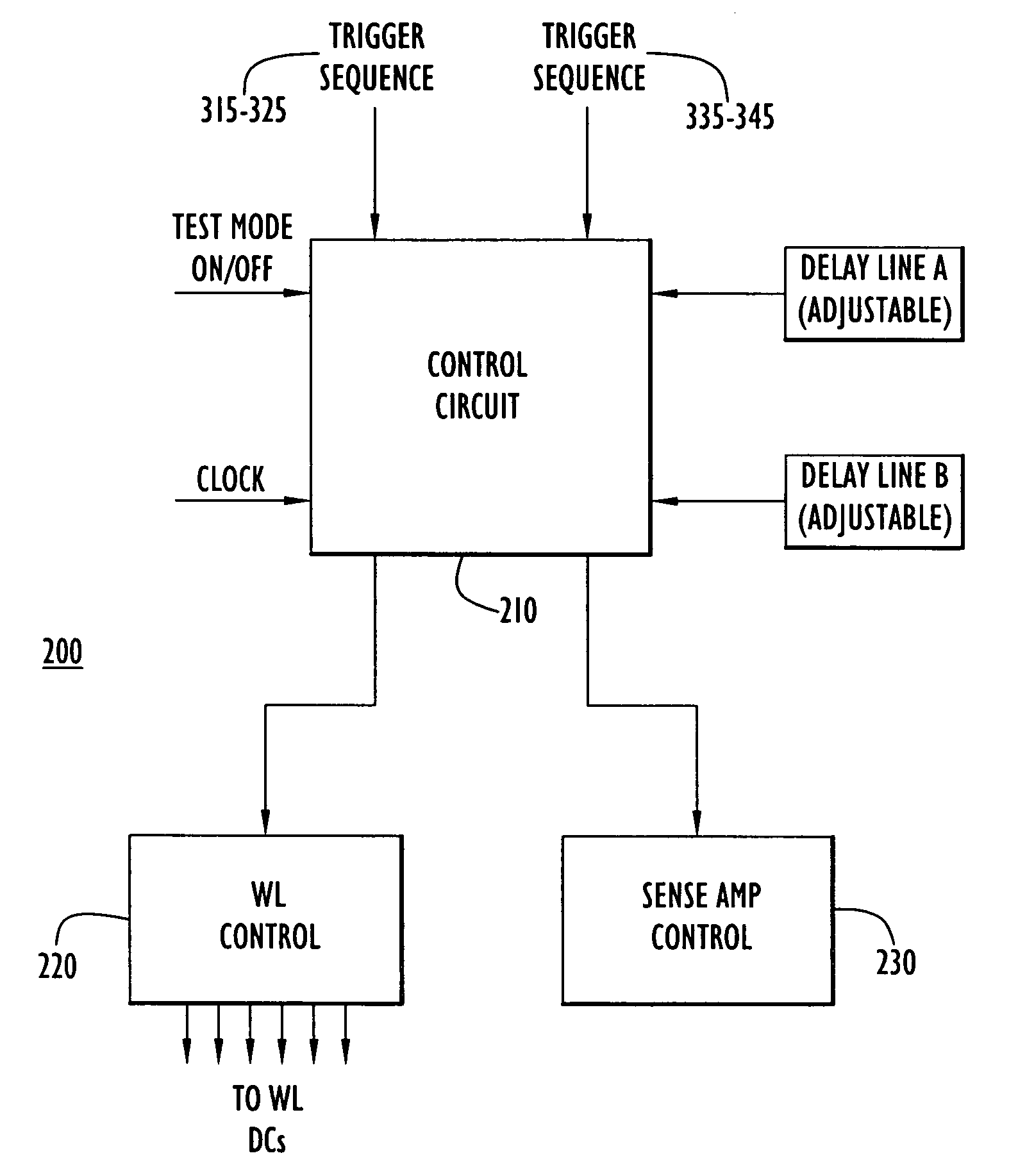
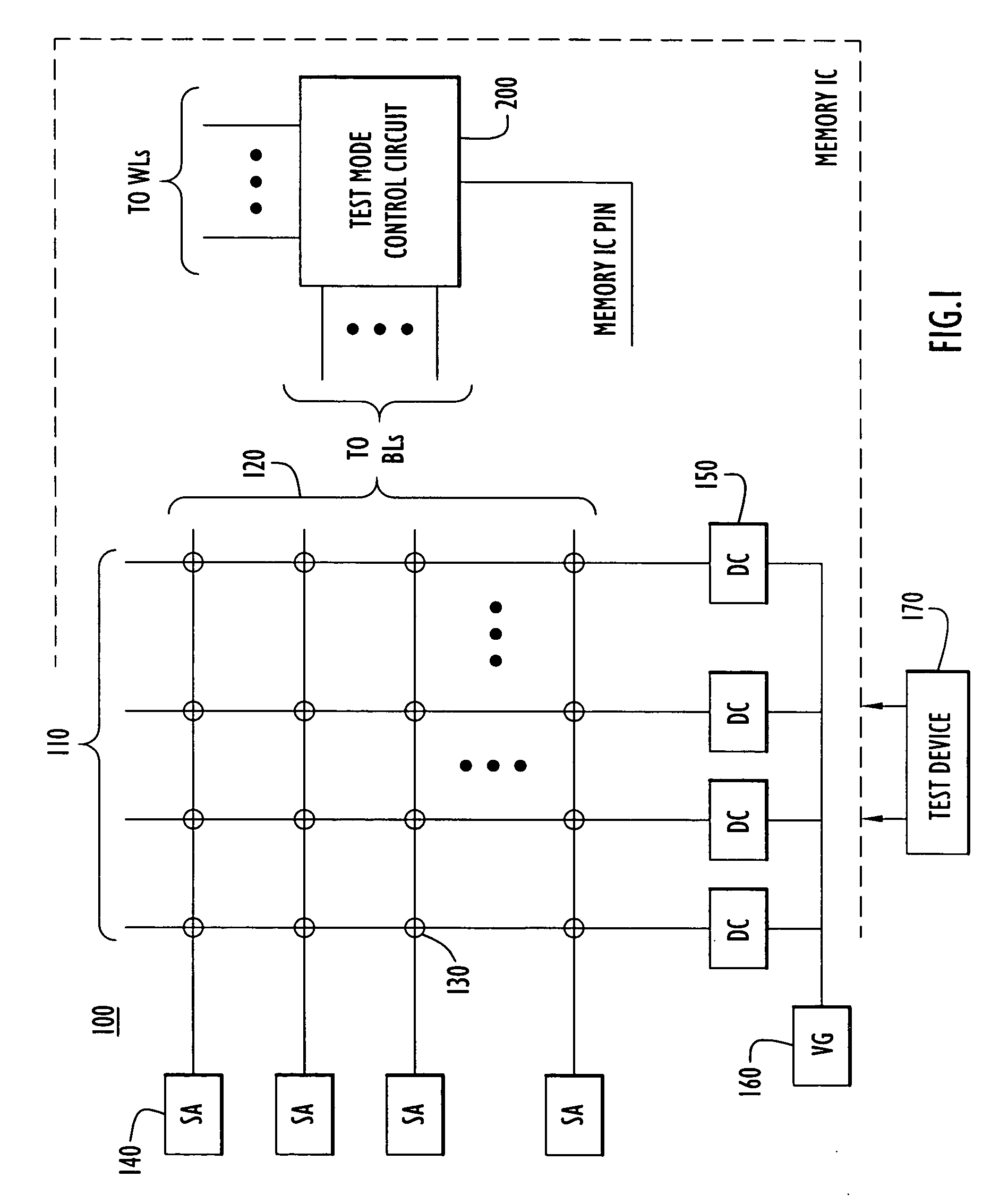
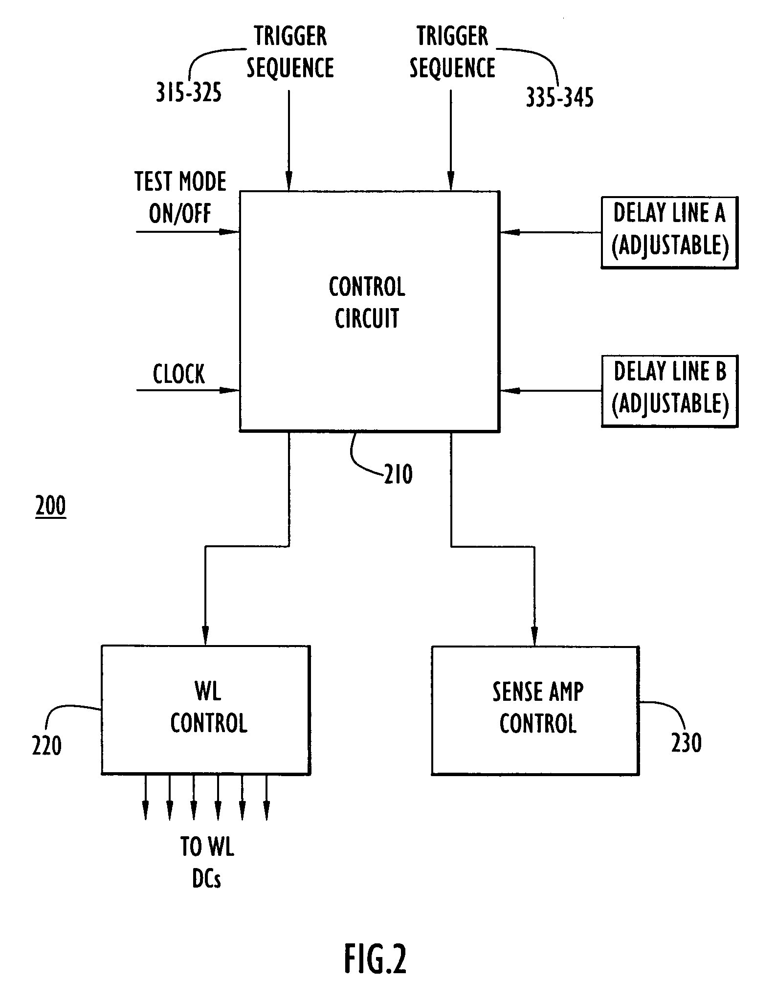
[0013] Referring first to FIG. 1, a portion or bank of a memory array is shown at reference numeral 100 that would be contained in a memory integrated circuit (IC) represented by the dotted line, such as a dynamic random access memory (DRAM) IC. There are a plurality of wordlines (WLs) 110 and a plurality of bitlines (BLs) 120 in a bank 100, and a plurality of banks in a memory IC. In a bank, the WLs 110 and BLs intersect at storage cells 130. There are many array configurations that are possible, and the test mode procedures described herein are not limited to the configuration shown in FIG. 1. Associated with the BLs 120 are sense amplifiers (SAs) 140. Associated with each WL are driver circuits (DCs) 150 that are used to activate and deactivate a corresponding WL. A voltage generator (VG) or source 160 is provided to supply the necessary voltages to activate and deactivate the WLs 110. Depending on some implementations, more than one VG may be needed for all of the WLs in a memor...


PUM


Abstract

A method, test mode circuit and system for a combined write window and retention test for a memory device that is faster than techniques heretofore known. The combined write window and retention test procedure involves controlling time intervals during which wordlines are activated and deactivated and bitlines are grounded or connected to a bitline high voltage such that the wordlines are activated while bitlines are either grounded or at the bitline high voltage. During a first time interval after the wordlines are activated a first value (e.g., 0 V) is written to storage cells associated with the activated wordlines. During a second time interval after a second activation of the wordlines, a second value (a non-zero logic “1” V) is written to storage cells associated with activated wordlines. The second time interval has a duration that establishes write window test conditions. After expiration of a third time interval corresponding to a retention time interval, the storage cells are read and a determination is made whether a storage cell has passed or failed a combined write window and retention test based on a value read from the storage cell.

Description

FIELD OF THE INVENTIONS [0001] This invention relates to testing semiconductor wafers, and more particularly to reducing the time required for testing semiconductor memory integrated circuit (IC) devices, such as dynamic random access memories (DRAMs). BACKGROUND OF THE INVENTION [0002] In the complex manufacturing steps of semiconductor memory devices, such as DRAMs, defects may occur and it is critical to test for and discover such defects before final production and shipment. Two tests that are commonly performed are the “write window” test and the “retention test.” As is known in the art, the write window test consists of writing a signal to a memory cell in such a manner so as to cut short the time that the cell is permitted to otherwise charge completely. For example, the cell may be permitted to charge to only two-thirds of its final charged value. Measurements are then made concerning surrounding resistive and other properties under these conditions. A retention test consist...

Claims


Application Information

Patent Timeline
IPC IPC(8): G11C29/00
CPCG11C11/401G11C29/50G11C29/50012G11C29/50016
Inventor NIERLE, KLAUS
Owner INFINEON TECH AG
Why Eureka
Try Eureka