Light emitting display

a technology of light-emitting displays and capacitors, applied in the direction of instruments, static indicating devices, etc., can solve the problems of insufficient charging time considering a line time of tens of s, relatively long charging time of data signals in capacitors, and low applied curren

Active Publication Date: 2006-06-29
SAMSUNG DISPLAY CO LTD
View PDF13 Cites 52 Cited by
  • Summary
  • Abstract
  • Description
  • Claims
  • Application Information

AI Technical Summary

Benefits of technology

[0008] It is therefore an object of the present invention

Problems solved by technology

In current programming type pixel circuit, the current needs to be minutely controlled, so that it takes relatively much time to charge the data signal in the capacitor.
However, there is not e

Method used


Image

  • Light emitting display
  • Light emitting display
  • Light emitting display

Examples


first embodiment

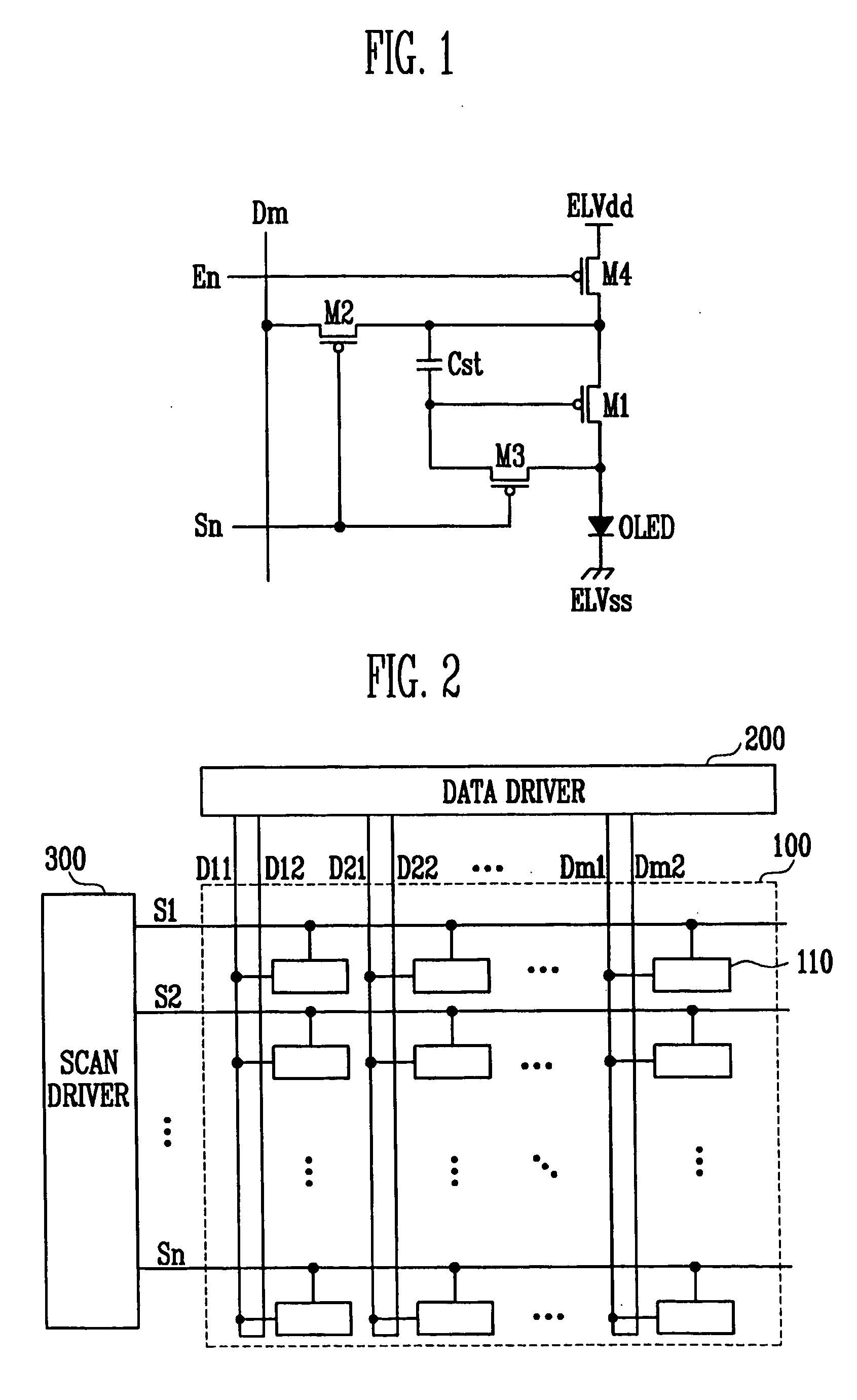
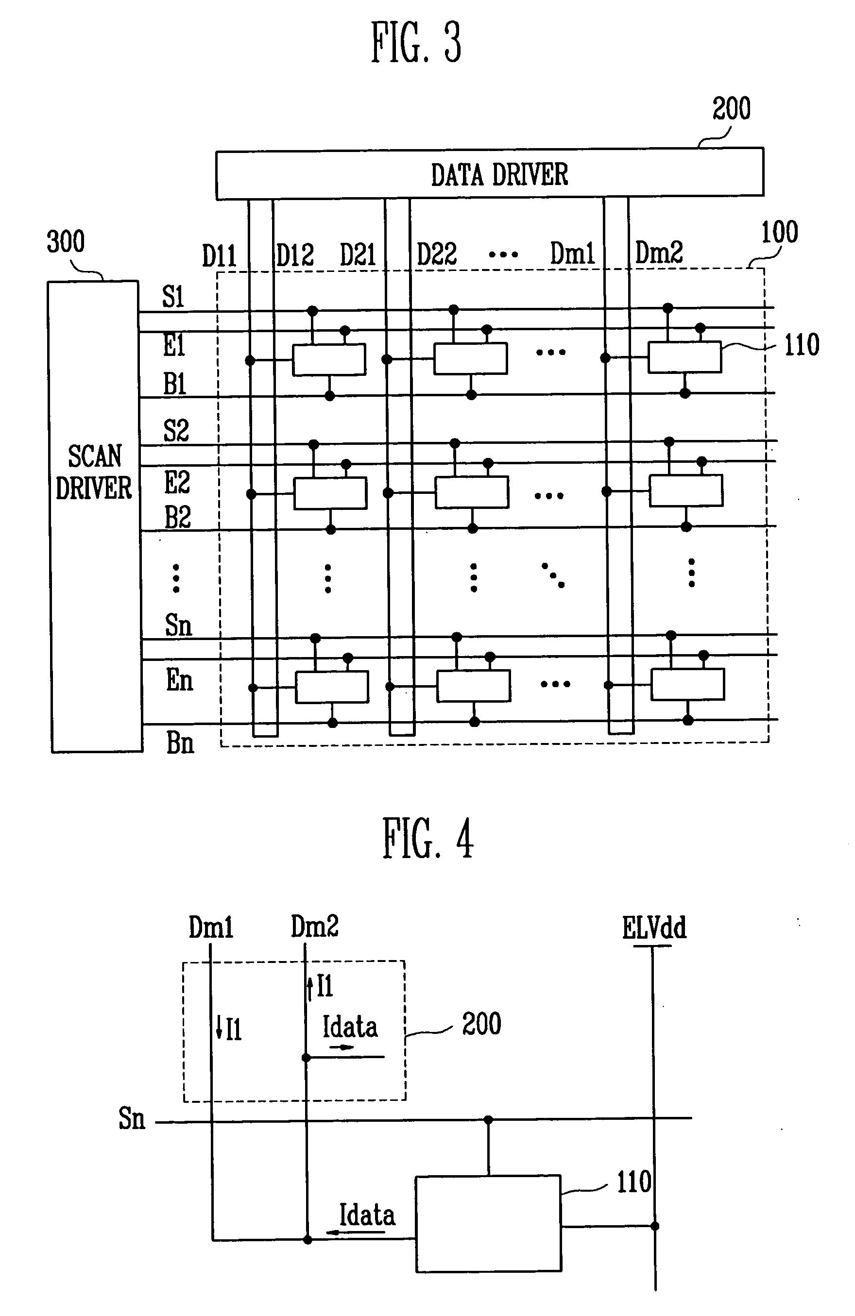
[0043] Turning to FIG. 3, FIG. 3 is a view of a layout diagram illustrating a light emitting display according to the present invention. Referring to FIG. 3, a light emitting display according to this embodiment of the present invention includes a pixel portion 100 that displays an image thereon, a data driver 200 that generates a data signal, and a scan driver 300 that generates a scan signal

[0044] The pixel portion 100 includes a plurality of pixels 110 that each include a light emitting devices and a pixel circuit. A plurality of scan lines S1, S2, . . . , Sn-1, Sn and a plurality of emission control lines E1, E2, . . . , En-1, En, which are arranged in a row direction, a plurality of data lines D1, D2 . . . , Dm-1, Dm arranged in a column direction, a plurality of power lines ELVdd that supply pixel power to the pixels 110, and a plurality of boost lines B1, B2, . . . , Bn-1, Bn that transmit a boosting signal to the pixels 110 are connected to the pixels 110. Each of the data l...

second embodiment

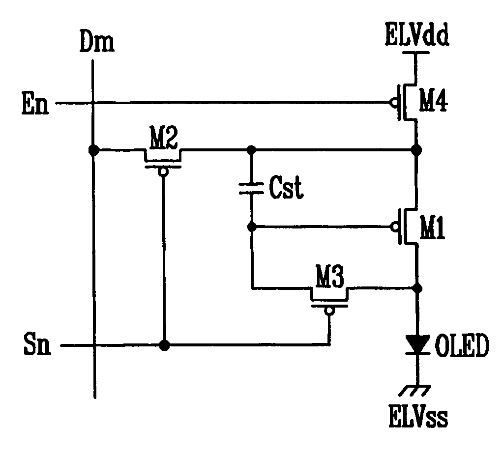
[0064]FIG. 8 is view of a circuit diagram illustrating the pixel 110 employed in the light emitting display of FIG. 2. Referring to FIG. 8, the pixel 110 includes the pixel circuit and the OLED. The pixel circuit includes transistors M1 through M4 and capacitor C1. Each of transistors M1 through M4 includes a source, a drain and a gate. Further, capacitor C1 includes a first electrode and a second electrode. In FIG. 8, transistors M1 through M4 are illustrated as being PMOS transistors. There is no physical difference between the source and the drain of each transistor, so that they can instead be called a first electrode and a second electrode. Further, the OLED is connected to transistor M4, and receives a current through transistor M4, thus generating light.

[0065] Regarding transistor M1, the source is connected to the power line ELVdd to receive the pixel power, the drain is connected to the OLED, and the gate is connected to node A. In transistor M1, a constant current flows fr...


PUM


Abstract

A light emitting display that includes a pixel portion having a plurality of pixels to display an image, a scan driver to supply a scan signal and an emission control signal to the pixel portion, and a data driver connected to a plurality of data lines each divided into a first data line through which a first current is supplied to the pixel, and a second data line through which a current having the same magnitude as the first current and a data current are induced from the pixel, wherein the data driver includes a current applying circuit to generate the first current, supply the first current to the pixel through the first data line, and receive the first current from the pixel through the second data line; and a data driving integrated circuit to induce the data current in the pixel through the second data line.

Description

CLAIM OF PRIORITY [0001] This application makes reference to, incorporates the same herein, and claims all benefits accruing under 35 U.S.C. §119 from an application earlier filed in the Korean Intellectual Property Office on 24 Dec. 2004 and there duly assigned Serial Nos. 2004-112525, 2004-112526 and 2004-112528, respectively. BACKGROUND OF THE INVENTION [0002] 1. Field of the Invention [0003] The present invention relates to a light emitting display, and more particularly, to a light emitting display that employs high current to enhance data programming speed, so that the display can have a large size and represent a high gradation. [0004] 2. Description of Related Art [0005] Various flat panel displays have recently been developed as alternatives to the relatively heavy and bulky cathode ray tube (CRT) display. The flat panel display includes a liquid crystal display (LCD), a field emission display (FED), a plasma display panel (PDP), a light emitting display, etc. [0006] The li...

Claims


Application Information

Patent Timeline
IPC IPC(8): G09G3/30
CPCG09G3/3241G09G3/325G09G3/3283G09G2300/0842G09G2300/0852G09G2300/0861G09G2310/0248G09G2310/027G09G2320/0223
Inventor CHOI, SANG-MOOKWON, OH-KYONG
Owner SAMSUNG DISPLAY CO LTD
Why Eureka
Try Eureka