Method for manufacturing electronic memory devices integrated in a semiconductor substrate including non-volatile memory matrix and associated circuitry

a semiconductor substrate and non-volatile memory technology, applied in the field of semiconductor memory, can solve the problems of affecting the dimensional and alignment performance required of the layers, the duv resist type shows a lower adhesion capacity to the underlying layers, and the standard process flow is altered to form these memory cells

Inactive Publication Date: 2006-07-06
STMICROELECTRONICS SRL
View PDF4 Cites 0 Cited by
  • Summary
  • Abstract
  • Description
  • Claims
  • Application Information

AI Technical Summary

Problems solved by technology

Moreover, this type of DUV resist shows a lower capacity of adhesion to the underlying layers whereon it is distributed (these latter being of nitride / oxide / poly or metal,) also because this layer is very sensitive to the presence of contaminating elements, such as amines, which are formed on the surface to be covered.
This problem is particularly evident when thicknesses of layers of 0.15 μm or lower are defined.
Although advantageous under several aspects, these approaches have the drawback of altering the standard process flow used to form these memory cells.
However, these layers are not always compatible with the dimensional and alignment performances required by the recent technologies used for forming current electronic memory devices.

Method used


Image

  • Method for manufacturing electronic memory devices integrated in a semiconductor substrate including non-volatile memory matrix and associated circuitry
  • Method for manufacturing electronic memory devices integrated in a semiconductor substrate including non-volatile memory matrix and associated circuitry
  • Method for manufacturing electronic memory devices integrated in a semiconductor substrate including non-volatile memory matrix and associated circuitry

Examples


Embodiment Construction

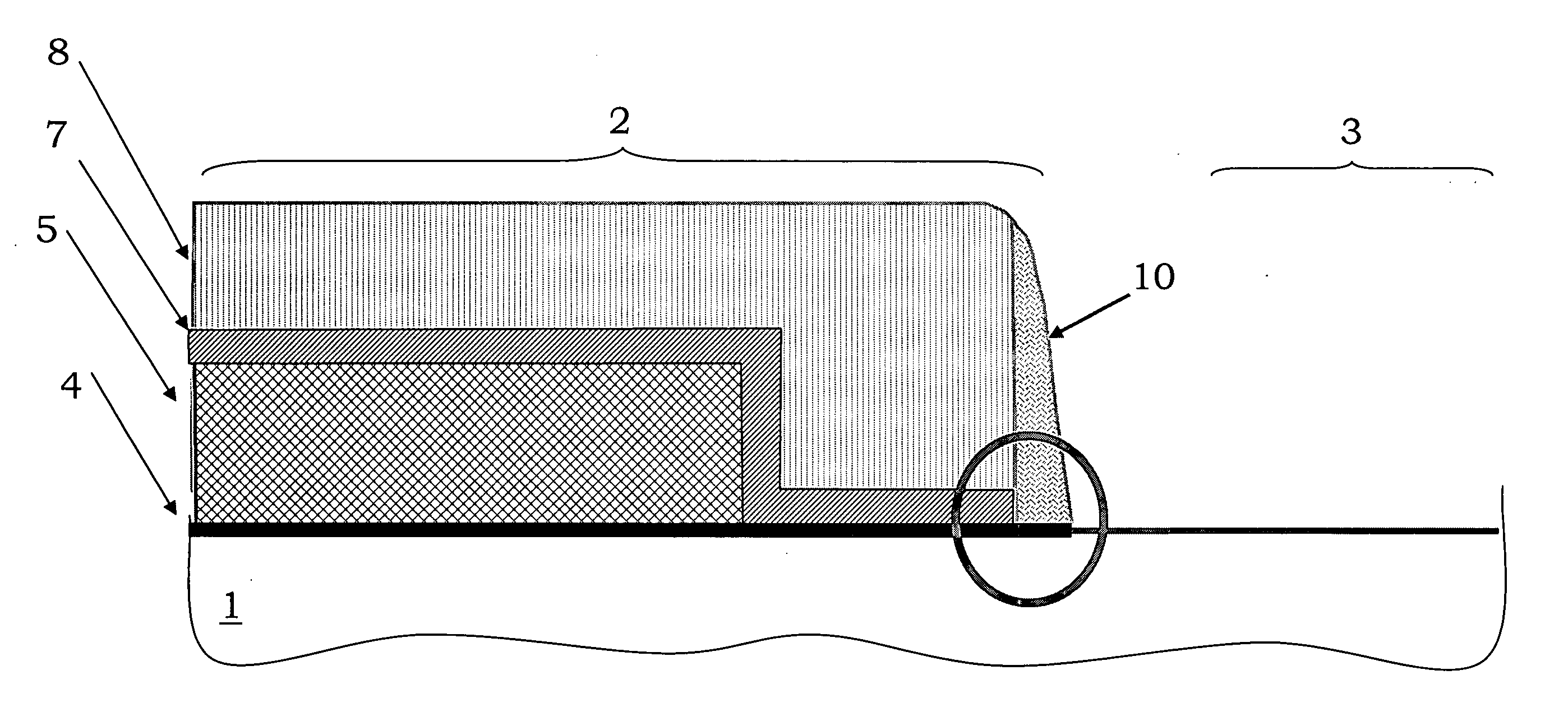
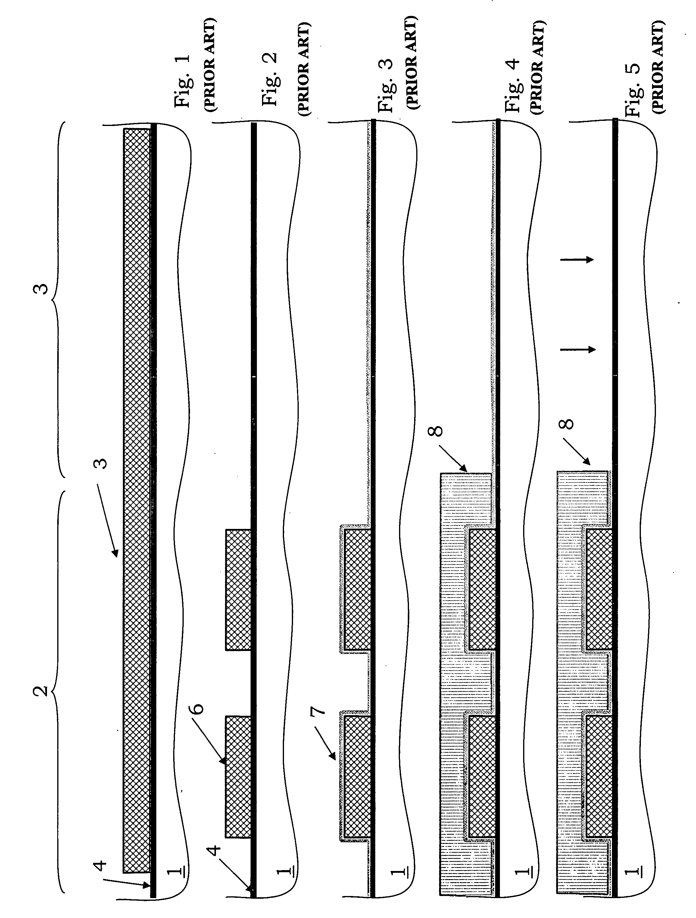
[0020] With reference to FIGS. 7 to 9 a method is described to manufacture electronic memory devices integrated on a semiconductor substrate 1, and comprising a non-volatile memory matrix 2 and associated circuitry. The method according to the invention is carried out with the following sequence of process steps. These steps described hereafter are not the complete process flow for the manufacturing of integrated circuits. The present invention can be put into practice together with the manufacturing techniques of the integrated circuits currently used in the field, and only those commonly used process steps being necessary for the understanding of the present invention are included.

[0021] The figures representing schematic views of portions of an integrated circuit during the manufacturing are not drawn to scale, but they are instead drawn so as to show the important characteristics of the invention. In the following description, the reference numbers used relative to the method a...


PUM


Abstract

The method is for manufacturing electronic memory devices on a semiconductor substrate including a non-volatile memory matrix and associated circuitry. The method includes forming a first insulation layer, a conductive layer and a second insulation layer. A resist mask is formed corresponding with the memory matrix to define a predetermined geometry in the second insulation layer. The exposed portions of the second insulation layer are isotropically etched. Also, a conformal protective layer is formed and removed via a second highly selective etching step to form portions of the conformal protective layer on side walls of the resist mask and of the insulation layer. A third isotropic etching step removes the insulation layers left exposed by the resist mask and by the portions of the protective layer. The portions of the conformal protective layer and of the resist mask are then removed.

Description

FIELD OF THE INVENTION [0001] The present invention relates to semiconductor memories, and particularly to a method for manufacturing electronic memory devices integrated on a semiconductor substrate and including a non-volatile memory matrix and associated circuitry. BACKGROUND OF THE INVENTION [0002] Conventional semiconductor-integrated memory electronic devices of the Flash Electrically Programmable Read Only Memory (Flash-EPROM) type include a plurality of non-volatile memory cells. Each single non-volatile memory cell comprises a MOS transistor wherein the gate electrode, placed above the channel region, is floating, i.e. it has a high impedance continuously towards all the other terminals of the same cell and the circuit wherein the cell is inserted. This floating gate is insulated from the channel region via a thin oxide layer called a tunnel oxide. [0003] The cell also comprises a second electrode, called a control gate, which is driven through suitable control voltages. Th...

Claims


Application Information

Patent Timeline
Patent Type & Authority Applications(United States)
IPC IPC(8): H01L21/336H01L21/461
CPCH01L21/28273H01L21/31144H01L27/115H01L27/11521H01L29/40114H10B69/00H10B41/30
Inventor PIVIDORI, LUCA
Owner STMICROELECTRONICS SRL
Why Eureka
Try Eureka