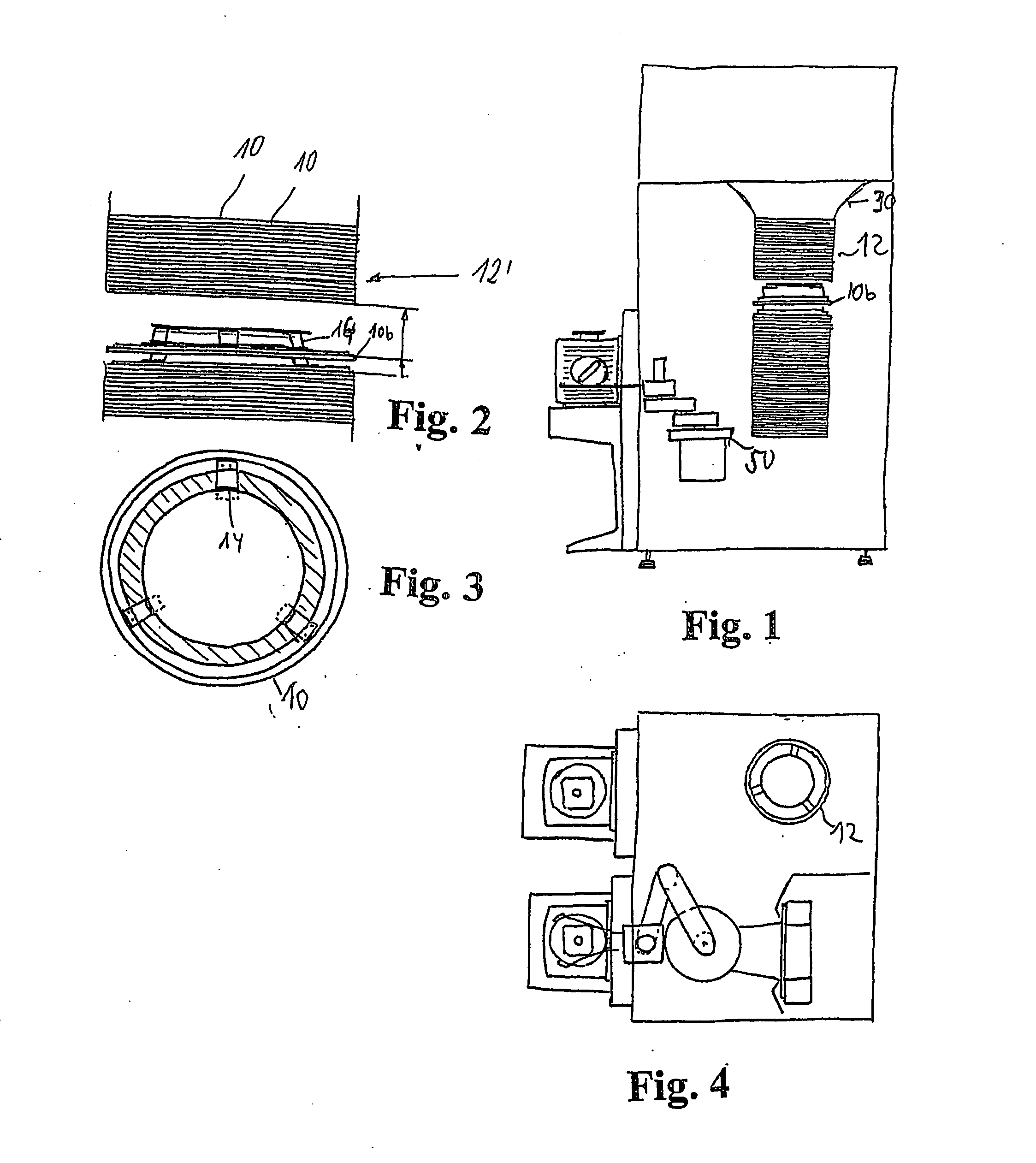
[0008] The object is accomplished by a device with a plurality of consecutive storage elements in a stacked direction, each of which is provided for accommodating at least one substrate. Each of the storage elements is provided with means for depositing the substrate. The storage elements have a stacking area, which is provided for arranging the respective storage element within a stack of storage elements. It is especially advantageous in this case if the respective distance between a plurality of consecutive storage elements and preferably between all consecutive storage elements can be changed from a storage distance to an access distance that is increased for this purpose. The result of this is that in the stored state, an as short as possible, so-called
pitch distance between consecutive storage elements and thus also substrates can be achieved. The storage distance is essentially only limited by a
minimum distance, which should be complied with, in order to guarantee that the surfaces of the substrates do not touch. Therefore, very tightly packed storage of wafers or other substrates is possible with the present invention. Nevertheless, the present invention makes possible the
advantage of being able to access each substrate contained in the closed storage means separately.
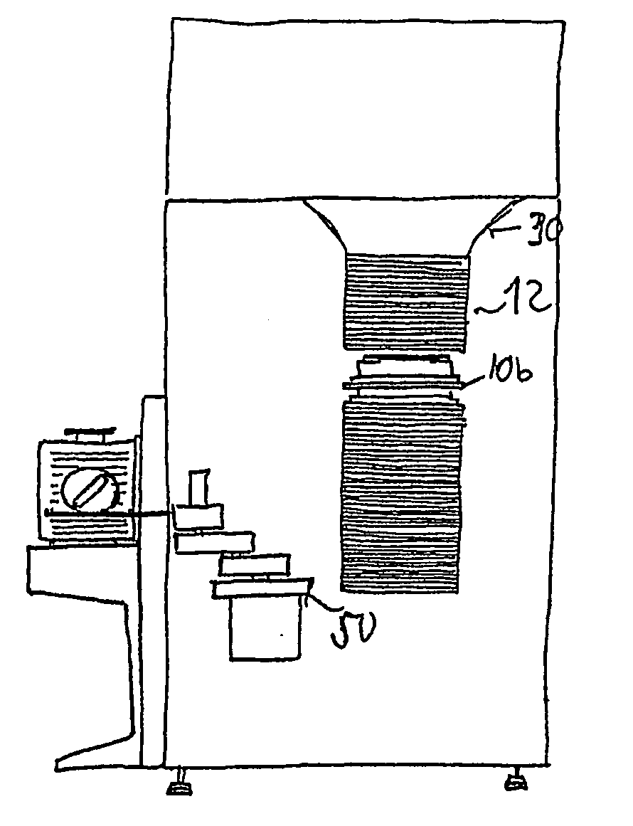
[0014] Consequently, it is also possible to embody the housing of the device by means of the storage elements themselves. Clean room conditions can be produced and maintained within the housing. An otherwise necessary, additional housing can be avoided by such an embodiment. Furthermore, the problem of an otherwise likewise necessary access opening in the housing and the positioning of the substrates to be removed or to be inserted in front of the access opening can thus be favorably avoided as well. Nevertheless, it may also be expedient, in certain embodiments of the present invention, to arrange the storage elements around a housing, which can be provided with an
insertion / removal opening for substrates and / or storage elements.
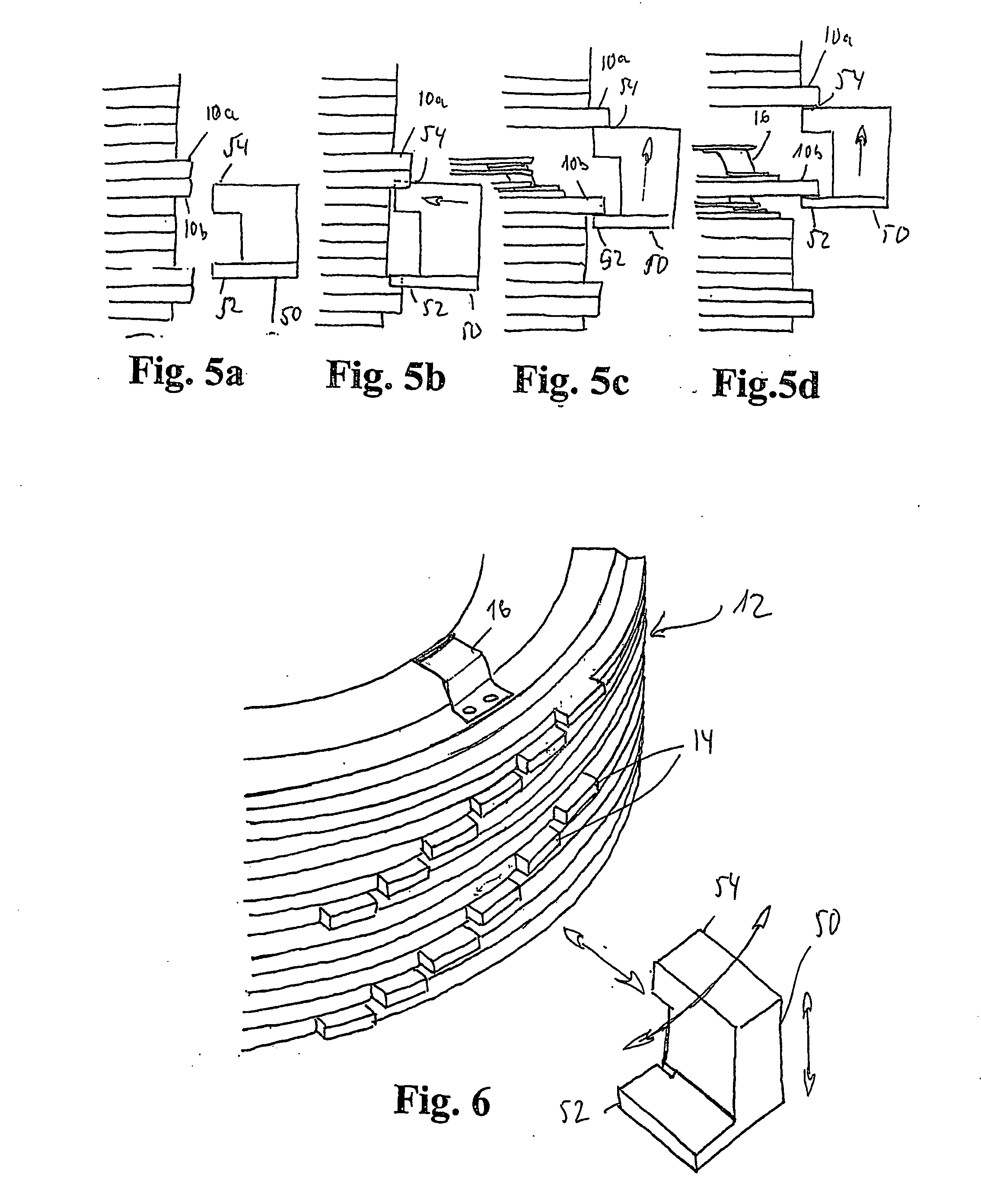
[0015] It is especially preferred here if the storage elements can be inserted or removed from the stack of storage elements separately. Particular advantages can then be achieved if a storage element can be removed or inserted at any point of the stack, without other storage elements having to be moved for this purpose beforehand or thereafter. This may, for example, be used for replacing a storage element with another storage element, transporting a substrate together with its storage element, or even for reducing or enlarging a stack. Consequently, the storage capacity may also be adapted to the respective conditions with very little effort. To achieve this, it may be expedient if the storage elements can be stacked on top of one another, without their having a detachable or undetachable connection to one another.
[0016] With such a solution, there is also the possibility of removing a substrate together with its storage element from the stack and transporting it within a
processing plant or a factory. Consequently, the number of necessary contacts between handling means and the respective substrate itself can be considerably reduced. Contacts of this type always hold the risk that the respective substrate is damaged.
[0018] The
tower or stack formed by means of a plurality of superimposed storage elements can be prone to
instability, especially when an access distance is formed between two storage elements. In order to avoid this, the device may be provided with stabilizing elements. Such stabilizing elements may be, for example, centering elements, which are attached at the storage elements and accurately align the storage elements in relation to one another. Lateral guide elements, which are arranged on the outside next to the storage elements and which prevent a tipping over of the
tower, are another possibility.
[0020] The extremely highly compressed storage of the substrates that can be achieved with the present invention is particularly advantageous in connection with transport devices, which are provided for transport outside of a factory since the costs and the technical effort for a transport increase with the size of the transport container. However, the use of such compact transport boxes or those transport boxes that have a markedly higher
accommodation capacity for substrates with the same dimensions as up to now may also be highly advantageous within a factory. In this connection, a transport container, in which only one storage element with its substrate can be accommodated, may also be advantageous. A storage element according to the present invention may or may not be provided with transport containers for transport within a factory on a
conveyor belt or another conveying means.

