Constant current circuit and flat display device
- Summary
- Abstract
- Description
- Claims
- Application Information
AI Technical Summary
Benefits of technology
Problems solved by technology
Method used
Image
Examples
embodiment 1
(1-3) Advantage of Embodiment 1
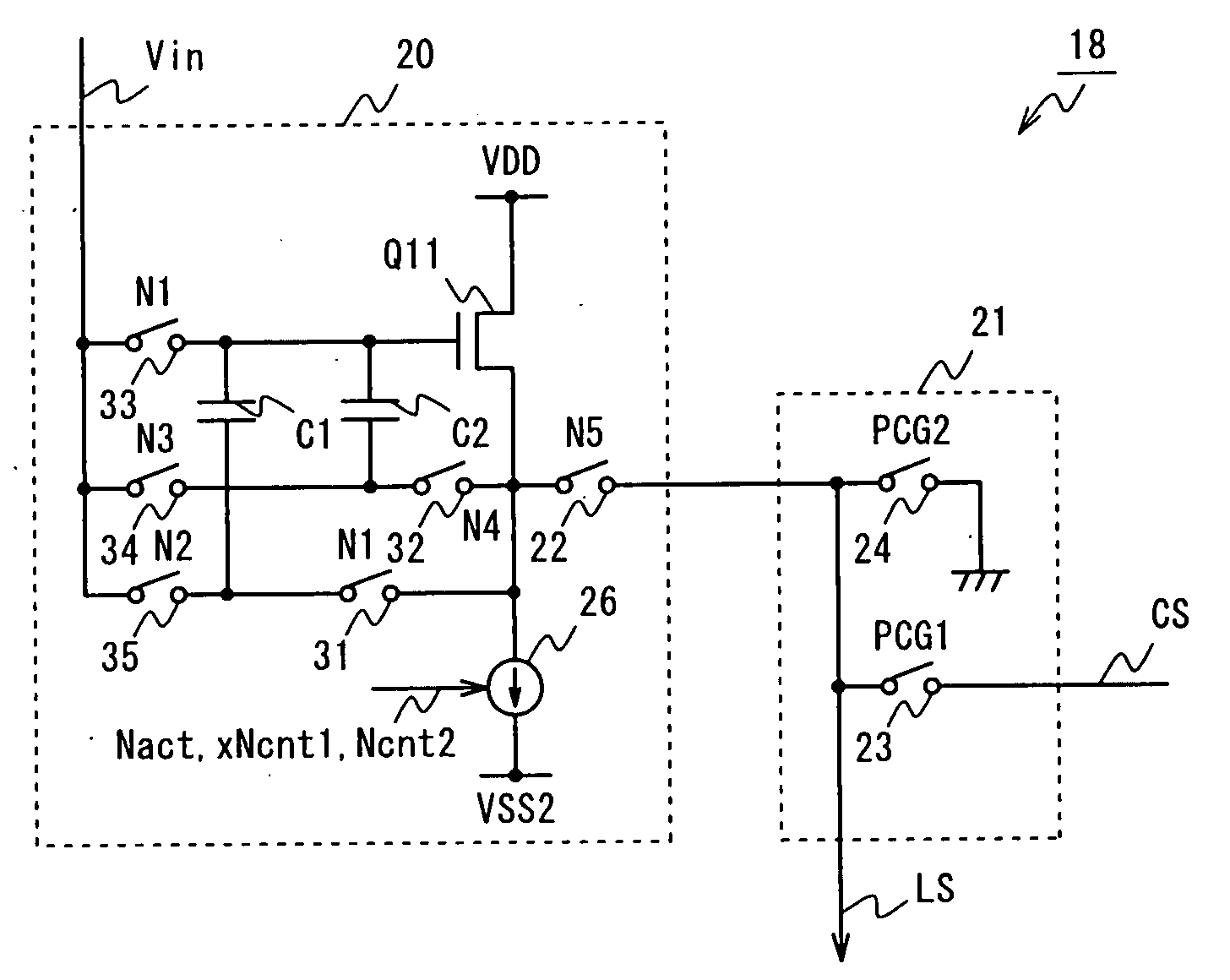
[0075] According to the above-mentioned construction, after a sampling capacitor is charged with a reference current and the gate-source voltage of a transistor due to the reference current is set in the sampling capacitor, the transistor is driven by the voltage of the sampling capacitor so as to function as a constant current circuit, so that variations can be reduced compared to conventional constructions.
[0076] In addition, by repeating processing associated with the sampling and processing which functions as the constant current circuit, it is possible to effectively avoid variations in output current due to voltage variations held in the sampling capacitor.
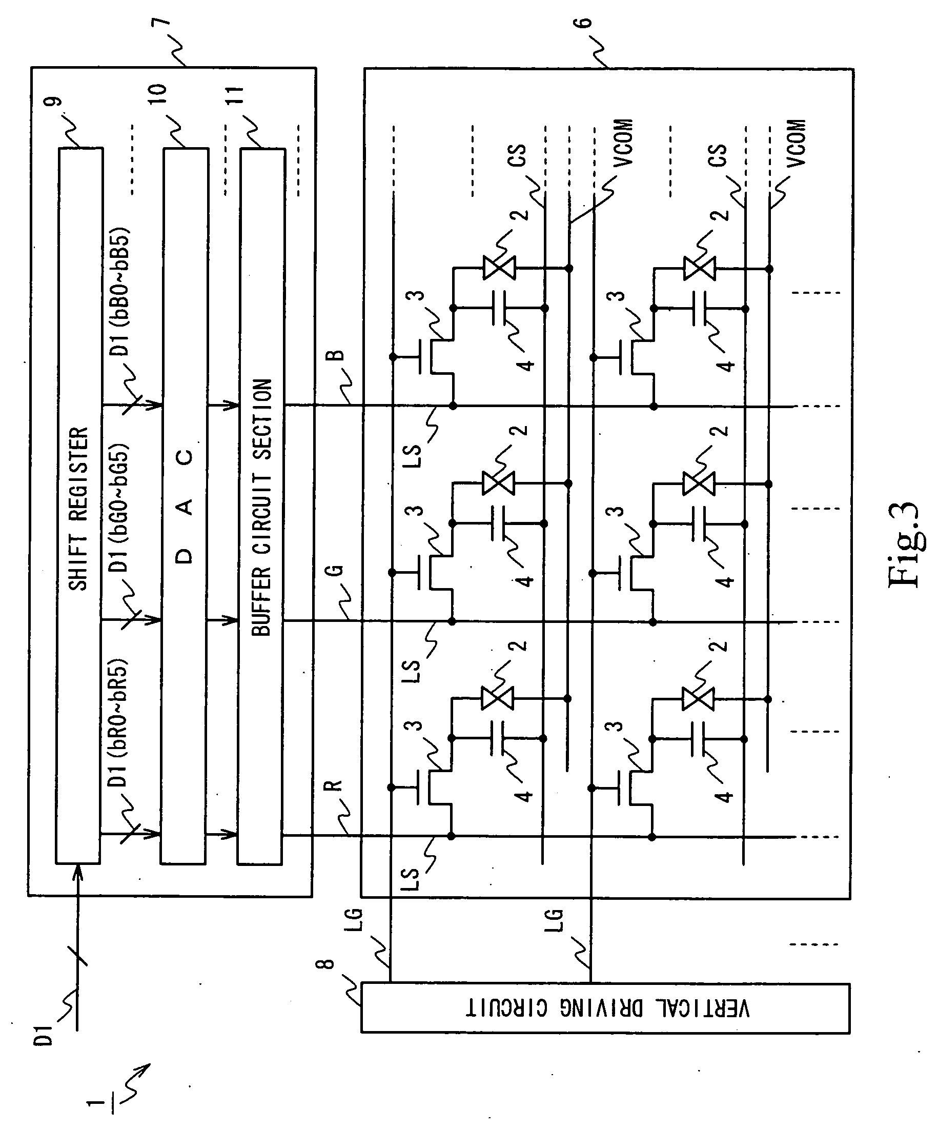
[0077] In addition, the above-mentioned construction is applied to a liquid crystal display, which is a flat display device, so that processing associated with voltage setting for the sampling capacitor is set in a period of precharge so as to set the voltage of the sampling capacitor and exe...
embodiment 2
(2) Embodiment 2
[0078]FIG. 14 is a block diagram showing the construction of an analog buffer circuit which is applied to a liquid crystal display according to Embodiment 2 of the present invention. An analog buffer circuit 40 is constructed with a PMOS source follower circuit in place of an analog buffer which is based on the NMOS source follower circuit according to Embodiment 1. Accordingly, in the liquid crystal display according to Embodiment 2, precharge processing associated with switching between ground potential and negative predetermined potential is executed in place of the precharge processing associated with the switching between the ground potential and the positive predetermined potential in the liquid crystal display device 1 according to Embodiment 1.
[0079] The analog buffer circuit 40 is constructed in the same manner as the analog buffer circuit 20 of Embodiment 1 except for its construction in which PMOS transistors are used in place of NMOS transistors, and exc...
embodiment 3
(3) Embodiment 3
[0082]FIG. 17 is a block diagram showing the construction of an analog buffer circuit which is applied to a liquid crystal display according to Embodiment 3 of the present invention. An analog buffer circuit 50 is constructed with a combination of an NMOS source follower circuit and a PMOS source follower circuit in place of the analog buffer based on the NMOS source follower circuit according to Embodiment 1. Accordingly, in the liquid crystal display according to Embodiment 3, precharge processing associated with switching between ground potential and negative predetermined potential is executed in place of the precharge processing associated with the switching between the ground potential and the positive predetermined potential in the liquid crystal display device 1 according to Embodiment 1.
[0083] As shown in FIG. 18, this analog buffer circuit is constructed with a combination of a source follower circuit using NMOS transistors according to Embodiment 1 and a ...
PUM
 Abstract
Description
Claims
Application Information


