

Display device and electronic device
a technology of electronic devices and display devices, applied in the field of display devices, can solve the problems of difficult to reduce the variation in the mobility and the threshold of the transistor, and the effect of reducing the characteristic variation is insufficien
Inactive Publication Date: 2011-09-29
SONY CORP
View PDF1 Cites 9 Cited by
- Summary
- Abstract
- Description
- Claims
- Application Information
AI Technical Summary
Benefits of technology
[0010]It is therefore desirable to provide a display device and an electronic device realizing improvement in display quality by suppressing luminance variations in a display face compared with an existing technique.
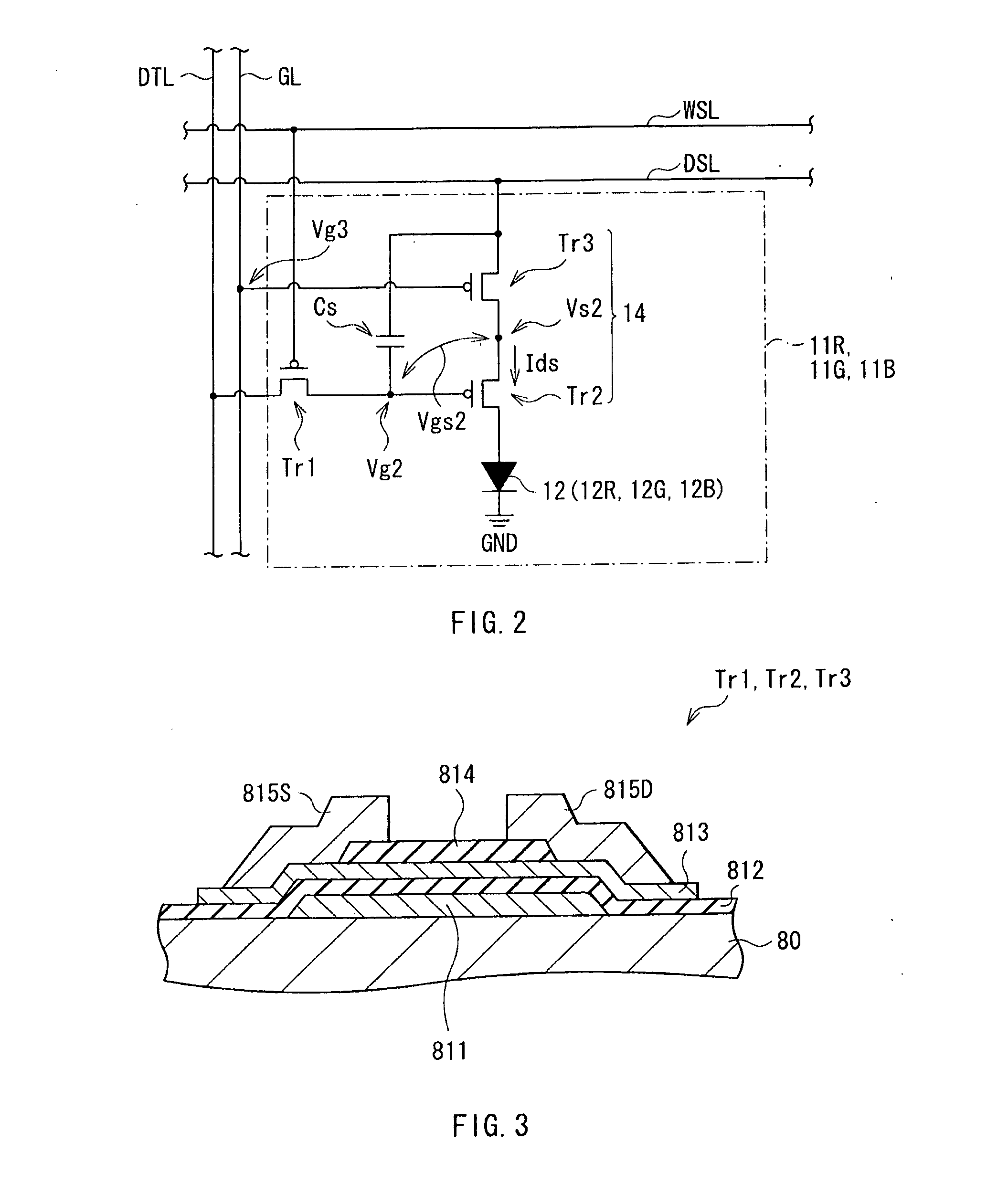
[0017]In the first display device and the first electronic device of an embodiment of the invention, in each pixel, the transistor for driving and the transistor for correction are connected to each other in series on a path between the power supply line and the light emitting element, and the gate voltage for correction to be applied to the gate of the transistor for correction via the gate line is set individually in each of unit regions in the display unit. Consequently, variations in the mobility and the threshold of the transistor for driving among the unit regions are reduced. Therefore, by reducing such variations caused by, for example, manufacture process, luminance variations in a display face are suppressed, and the display quality is improved.
[0018]In the second display device and the second electronic device of an embodiment of the invention, in each pixel, the transistor for driving is disposed on a path between the power supply line and the light emitting element, and the gate voltage for correction to be applied to the back gate of the transistor for driving via the gate line is set individually in each of unit regions in the display unit. Consequently, variations in the mobility and the threshold of the transistor for driving among the unit regions are reduced. Therefore, by reducing such variations caused by, for example, manufacture process, luminance variations in a display face are suppressed, and the display quality is improved.
Problems solved by technology
In the method of Japanese Unexamined Patent Application Publication No. 2004-212684, however, in principle, the characteristic variations in the drive transistors are not adjusted individually (arbitrarily) in each of the regions in the display face, so that the effect of reducing the characteristic variations is insufficient.
In the existing method, it is difficult to reduce variations in the mobility and the threshold of the transistor for driving caused by a manufacture process or the like, so that a method for reducing the variations is in demand.
Method used
View moreImage
Smart ImageViewing Examples

Examples
first embodiment (
1. First embodiment (example of a pixel circuit in which a correction transistor is disposed between a power supply line and a drive transistor)
second embodiment (
2. Second embodiment (example of a pixel circuit in which a drive transistor is disposed between a power supply line and a correction transistor)
third embodiment (
3. Third embodiment (example of applying gate voltage for correction is applied to the back gate of a drive transistor)
4. Modification (modification on the laser annealing direction)
Login to View More PUM
 Abstract
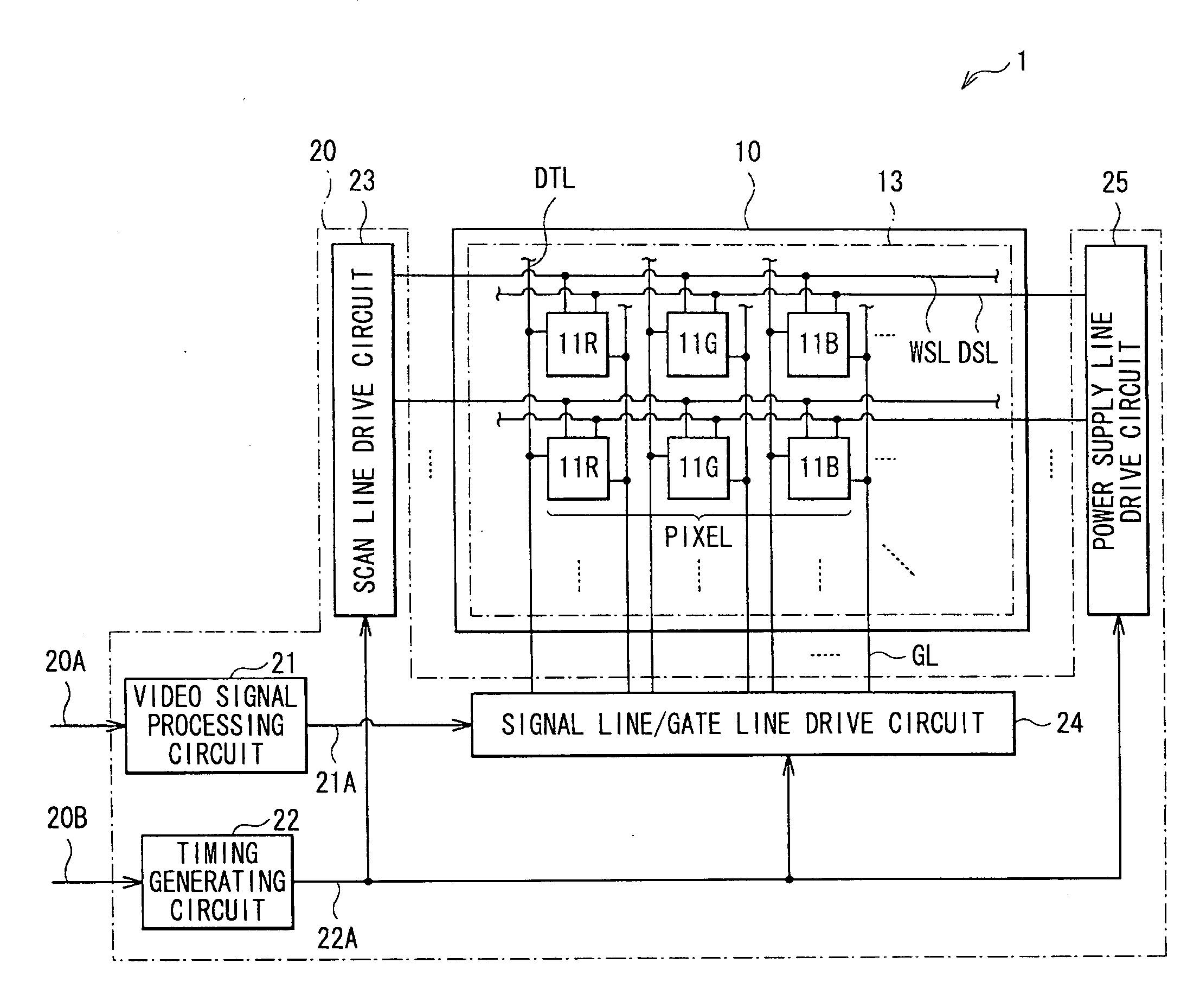
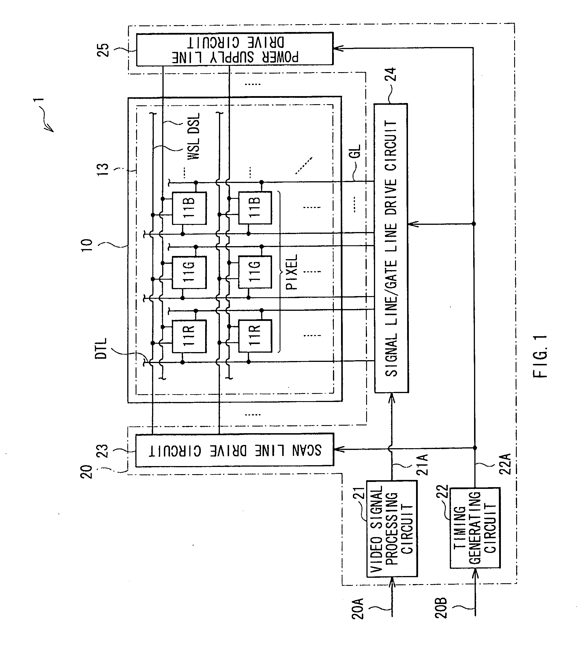
A display device includes: a display unit having a plurality of pixels each including a light emitting element, a drive transistor and a correction transistor, a scan line, a signal line, a power supply line and a gate line connected to the pixels; a scan line drive circuit applying a selection pulse to the scan line; and a signal line drive circuit writing a video signal to a pixel selected by the scan line drive circuit by applying a video signal voltage to the signal line. The drive transistor and the correction transistor are connected to each other in series on a path between the power supply line and the light emitting element in each of the pixels. Gate voltage for correction to be applied to the gate of the correction transistor via the gate line is set individually in each of unit regions in the display unit.
Description
BACKGROUND OF THE INVENTION[0001]1. Field of the Invention[0002]The present invention relates to a display device constructed by using light emitting elements such as organic EL (Electro Luminescence) elements and an electronic device having such a display device.[0003]2. Description of the Related Art[0004]In recent years, in the field of a flat panel display (FPD), attention to an organic EL display device is increasing. An organic EL display device is, different from a liquid crystal display (LCD), a device using light emitting elements and, therefore, does not require a backlight in principle. It is consequently advantageous more than an LCD from the viewpoint of thinness and higher luminance. In particular, in an organic EL display device of the active matrix type in which a switching element such as a TFT (Thin Film Transistor) is provided for each pixel, by making each pixel held lighted (lighted by making voltage retained in a capacitor), power consumption is kept low, and i...
Claims
Login to View More Application Information
Patent Timeline
 Patent Type & AuthorityApplications(United States)
IPC IPC(8): G09G3/30G09G5/00H04N5/70H05B44/00
CPCG09G3/3233G09G2300/0819G09G2300/0842G09G2360/147G09G2300/0885G09G2320/0233G09G2320/043G09G2300/0861H10K59/131
InventorTATARA, SATOSHIUCHINO, KATSUHIDE
OwnerSONY CORP