Semiconductor device and a method of fabricating a semiconductor device

a semiconductor and semiconductor technology, applied in the field of semiconductor devices, can solve the problems of difficult sputtering of conformal layers on the sidewall of the trench, the density is relatively low, and the signal interruption caused by crosstalk between wiring is subject to closer examination

Inactive Publication Date: 2006-07-13
KK TOSHIBA
View PDF8 Cites 32 Cited by
  • Summary
  • Abstract
  • Description
  • Claims
  • Application Information

AI Technical Summary

Problems solved by technology

Along with the miniaturization of semiconductor devices, transmission delays and signal interruption by crosstalk between wiring have become a subject for closer examination.
However, the miniaturization of integrated circuits makes it difficult to deposit conformal layers on a sidewall of the trench by sputtering.
However, since the porous low k dielectric includes many pores in the dielectric, density is relatively low and is easily affected by atmospheric conditions.
Consequently, leakage of the wiring and an increase in wiring capacitance may occur.
However, since the barriers deposited by CVD or ALD have poor adhesion strength, the barriers may peel off after fabrication.

Method used


Image

  • Semiconductor device and a method of fabricating a semiconductor device
  • Semiconductor device and a method of fabricating a semiconductor device
  • Semiconductor device and a method of fabricating a semiconductor device

Examples


first embodiment

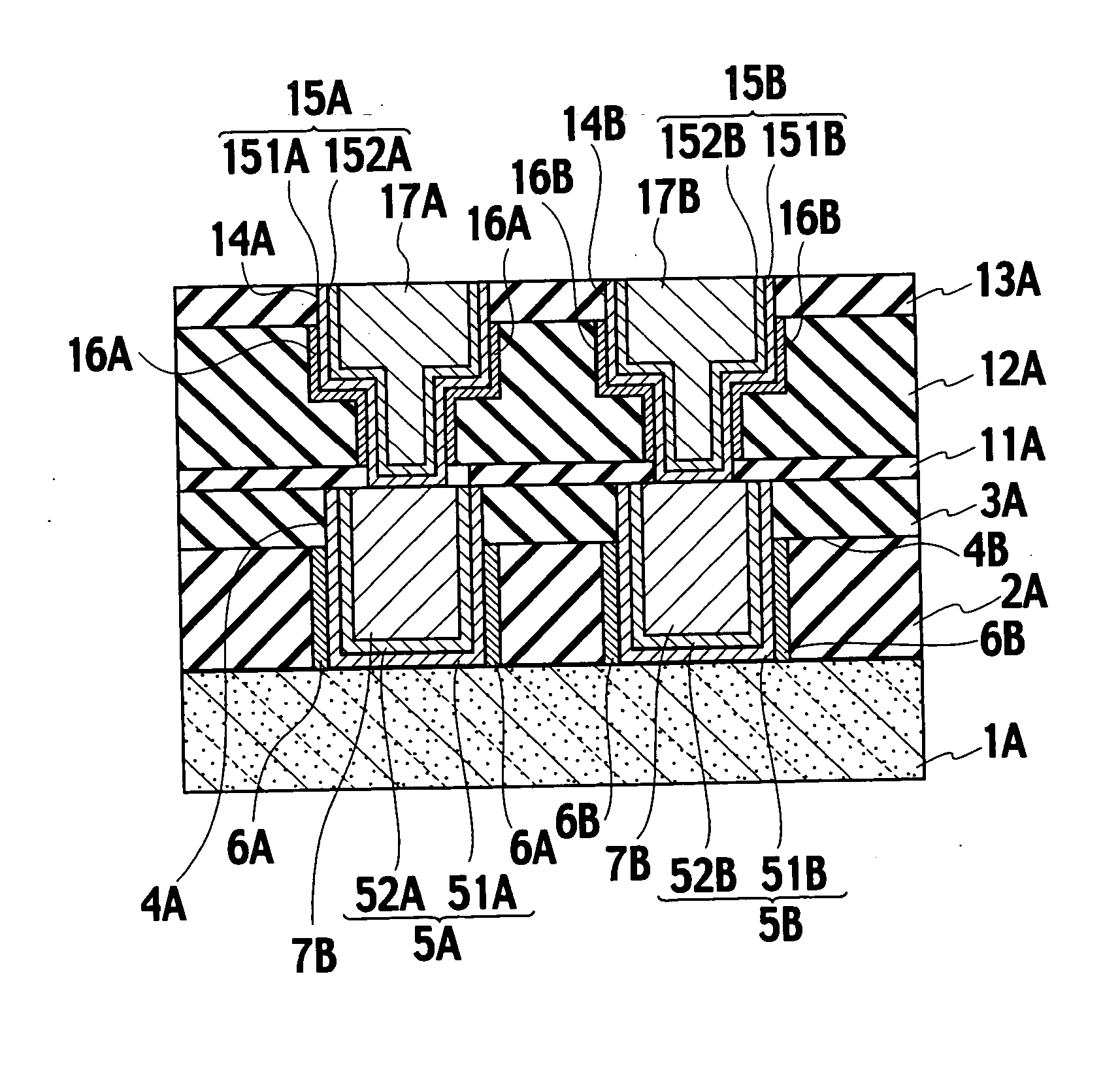
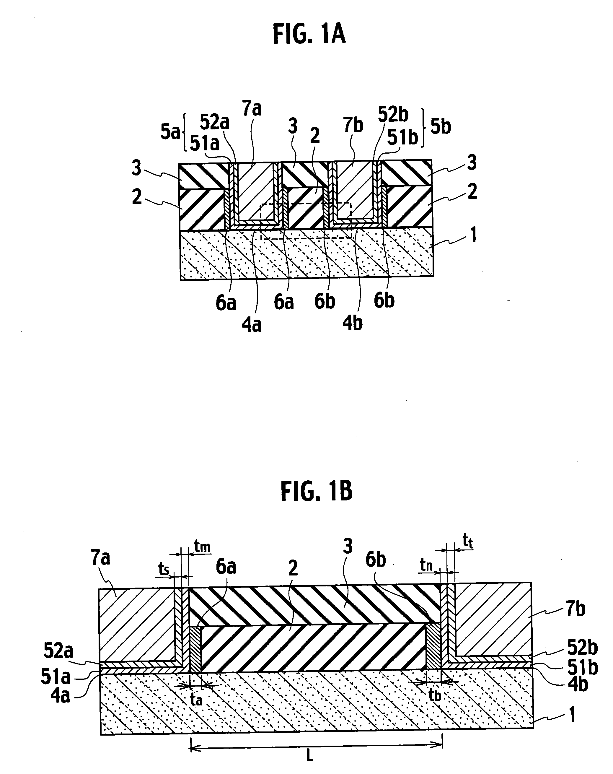
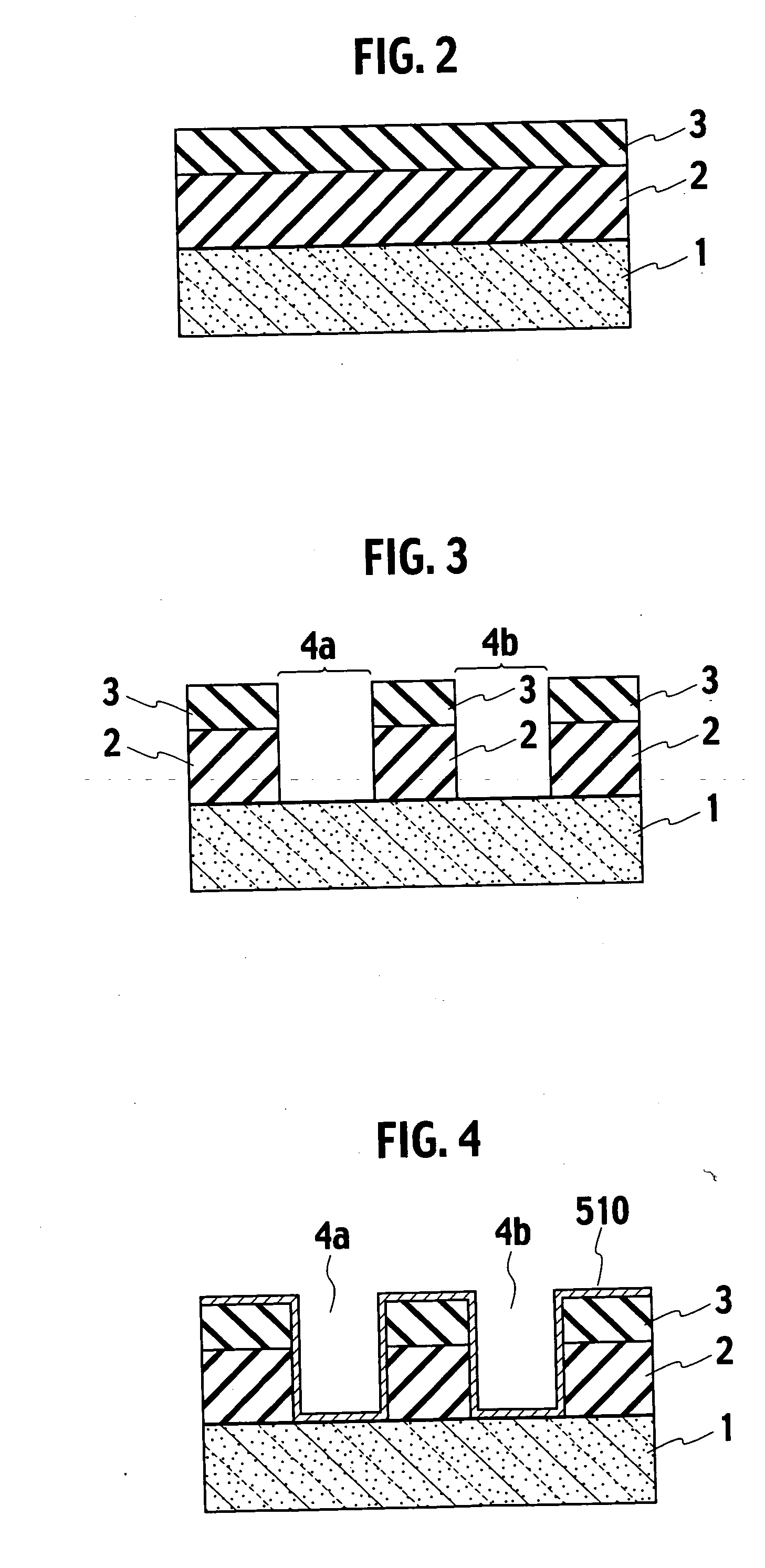
[0018] As shown in FIG. 1, a semiconductor device according to the first embodiment of the present invention includes a semiconductor substrate 1, a porous low k dielectric 2 having trenches 4a, 4b and disposed on the semiconductor substrate 1, barrier layers 5a, 5b provided on a surface of the trenches 4a, 4b, metal diffused regions 6a, 6b provided in the porous low k dielectric 2 and in contact with the barrier layers 5a, 5b, and first conductors 7a, 7b embedded in the trenches 4a, 4b in contact with the barrier layers 5a, 5b.

[0019] A stopper film 3, which is made from insulative material, may be disposed on the porous low k dielectric 2. A part of the barrier layers 5a, 5b and the conductor 7a, 7b may be formed in the stopper film 3.

[0020] In FIG. 1A, a semiconductor device fabricated by damascene processes is illustrated as an example of a semiconductor device according to the first embodiment. In FIG. 1A, transistors, isolation regions located adjacent to the semiconductor su...

second embodiment

[0042] As shown in FIG. 7, a semiconductor device according to the second embodiment of the present invention is different from the first embodiment in that the barrier layers 5a, 5b further include a third barrier films 53a, 53b provided on a surface of the second barrier films 52a, 52b.

[0043] The third barrier films 53a, 53b are conductive films having lower film density than the second barrier films 52a, 52b . The third barrier films 53a, 53b have microscopic asperities on surfaces thereof. A film thickness tu, tv of the third barrier film 53a, 53b in contact with the sidewalls of the second barrier films 52a, 52b may be in a range of from about 1 nm to about 3 nm. The third barrier films 53a, 53b can be made from Ti, Nb, Ta, Ru, W, and compounds such as alloys, nitrides, oxides, and carbides, which are made from at least two materials selected from above materials. Other elements of the second embodiment are substantially the same as those of the semiconductor device as shown i...


PUM

PropertyMeasurementUnit
dielectric constantaaaaaaaaaa
thicknessaaaaaaaaaa
thicknessaaaaaaaaaa

Abstract

A semiconductor device includes a semiconductor substrate; a porous low k dielectric disposed on the semiconductor substrate having a plurality of trenches therein, the porous low k dielectric having an effective dielectric constant of 3.0 or less; a plurality of barrier layers provided on each surface of the trenches, each of the barrier layers including a plurality of films having different film densities; a plurality of metal diffused regions provided in the porous low k dielectric and contacting the barrier layers; and a first conductor embedded in one of the trenches in contact with one of the barrier layer.

Description

CROSS REFERENCE TO RELATED APPLICATIONS AND INCORPORATION BY REFERENCE [0001] This application is based upon and claims the benefit of priority from the prior Japanese Patent Applications No. P2005-002637, filed on Jan. 7, 2005; the entire contents of which are incorporated herein by reference. BACKGROUND OF THE INVENTION [0002] 1. Field of the Invention [0003] The present invention relates to a semiconductor device, more specifically to a semiconductor device including a porous low k dielectric material as an interlayer dielectric. [0004] 2. Description of the Related Art Along with the miniaturization of semiconductor devices, transmission delays and signal interruption by crosstalk between wiring have become a subject for closer examination. Copper (Cu), which has a lower resistivity than aluminum (Al), has been adopted as conductive materials and a method for suppressing resistance by 30% has been employed. A low-k dielectric having a lower dielectric constant than a silicon oxi...

Claims


Application Information

Patent Timeline
Patent Type & Authority Applications(United States)
IPC IPC(8): H01L21/44H01L23/48
CPCH01L21/76801H01L21/76844H01L21/76846H01L21/76867H01L23/5222H01L2924/0002H01L23/53238H01L23/53295H01L2924/00
Inventor HIGASHI, KAZUYUKI
Owner KK TOSHIBA
Why Eureka
Try Eureka