

Circuit modeling and selective deposition
a circuit modeling and selective deposition technology, applied in the field of ink jet printing of electrical components, can solve the problems of inability to mount devices on internal layers, inability to produce well-defined features with good electrical properties, and insufficient approaches to date to achieve well-defined features
- Summary
- Abstract
- Description
- Claims
- Application Information
AI Technical Summary
Benefits of technology
Problems solved by technology
Method used
Image

Examples
Embodiment Construction
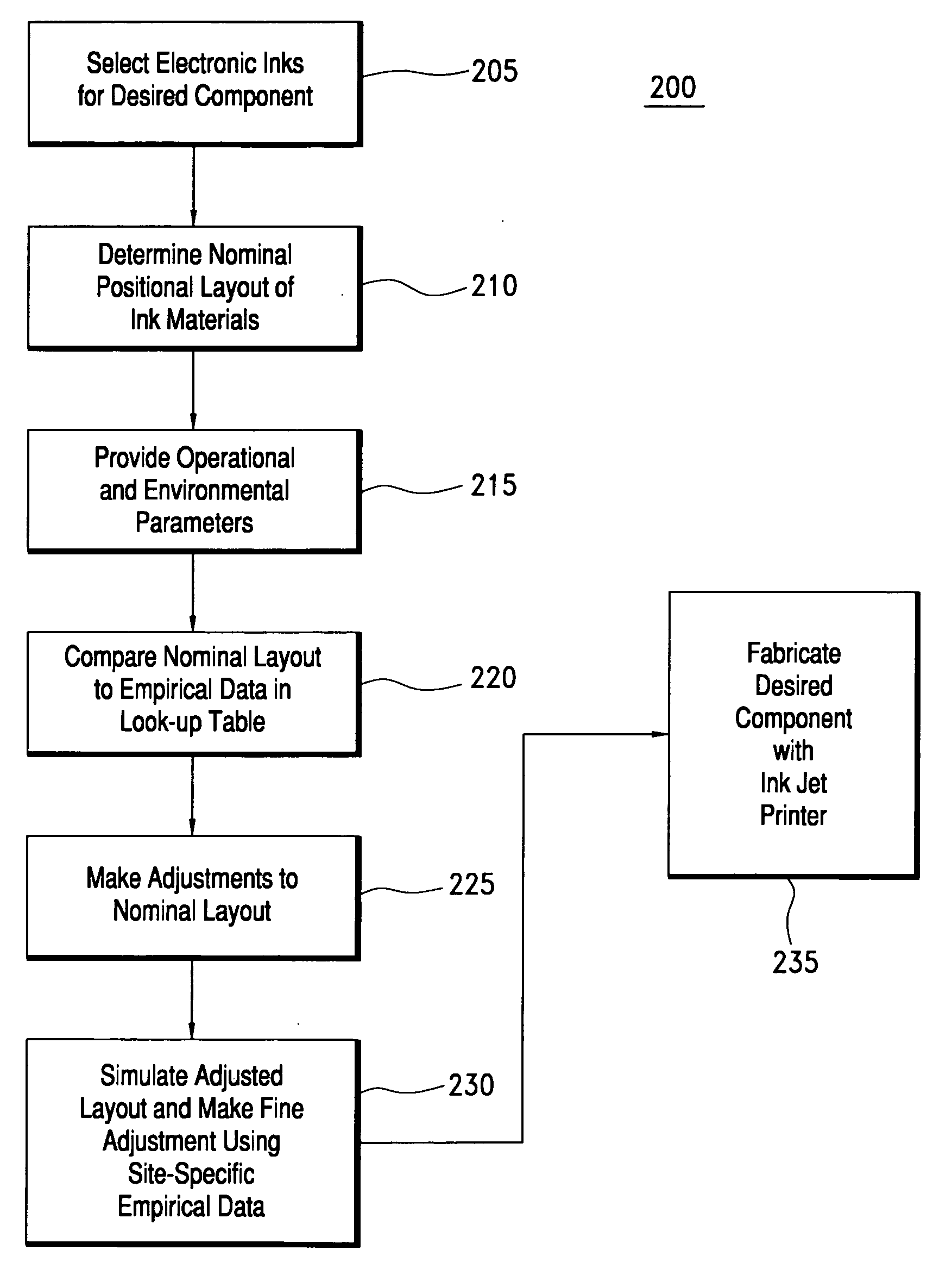
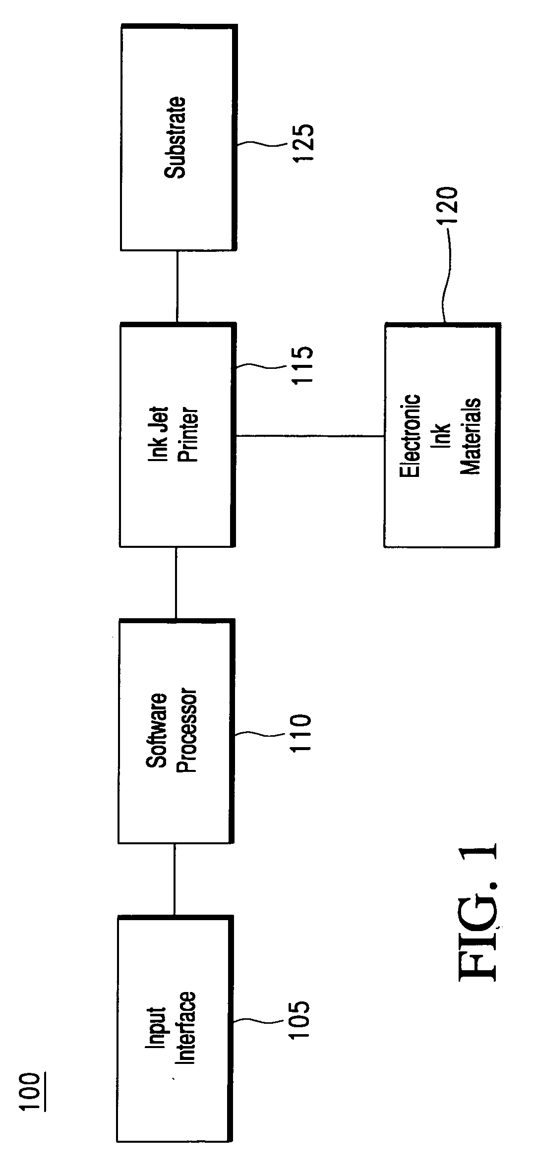
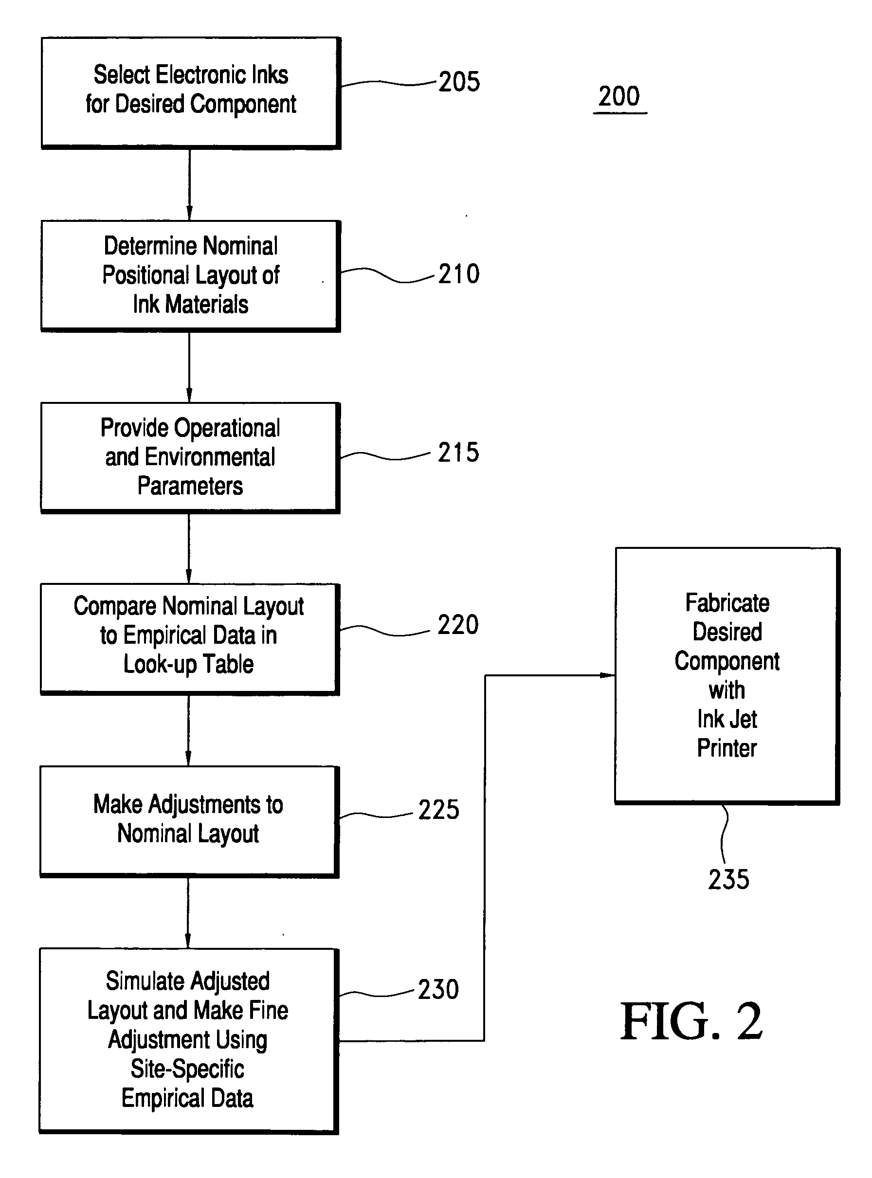
[0025] In an application of inkjet printing of electrical circuit elements onto a substrate, PCB or other layout tool software can be designed to allow for the input of a variety of requirements for a conductor, a dielectric, or an electrical component. These requirements may relate to such aspects as: 1) maximum level of current that will flow in the conductor, 2) maximum allowable voltage drop across the conductor in the application, 3) frequency of the signal that the conductor is carrying, 4) maximum allowable temperature rise of the conductor due to current transfer or frequency, 5) receiver minimum acceptable high voltage value, 6) receiver maximum acceptable low voltage value, 7) rise and fall time of a driven signal, 8) minimum and maximum voltage level of the driven signal, 9) desired impedance of a trace, 10) desired resistance of the trace, 11) acceptable overshoot and undershoot values that are allowable at the drive and receiver, 12) capacitance range, and 13) inductanc...
PUM
 Abstract
Description
Claims
Application Information