Device for the low-deformation replaceable mounting of an optical element
- Summary
- Abstract
- Description
- Claims
- Application Information
AI Technical Summary
Benefits of technology
Problems solved by technology
Method used
Image
Examples
Embodiment Construction
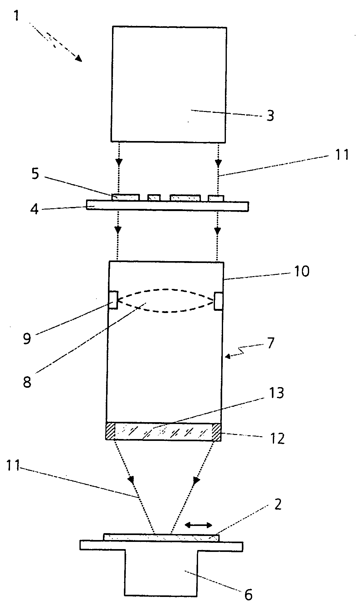
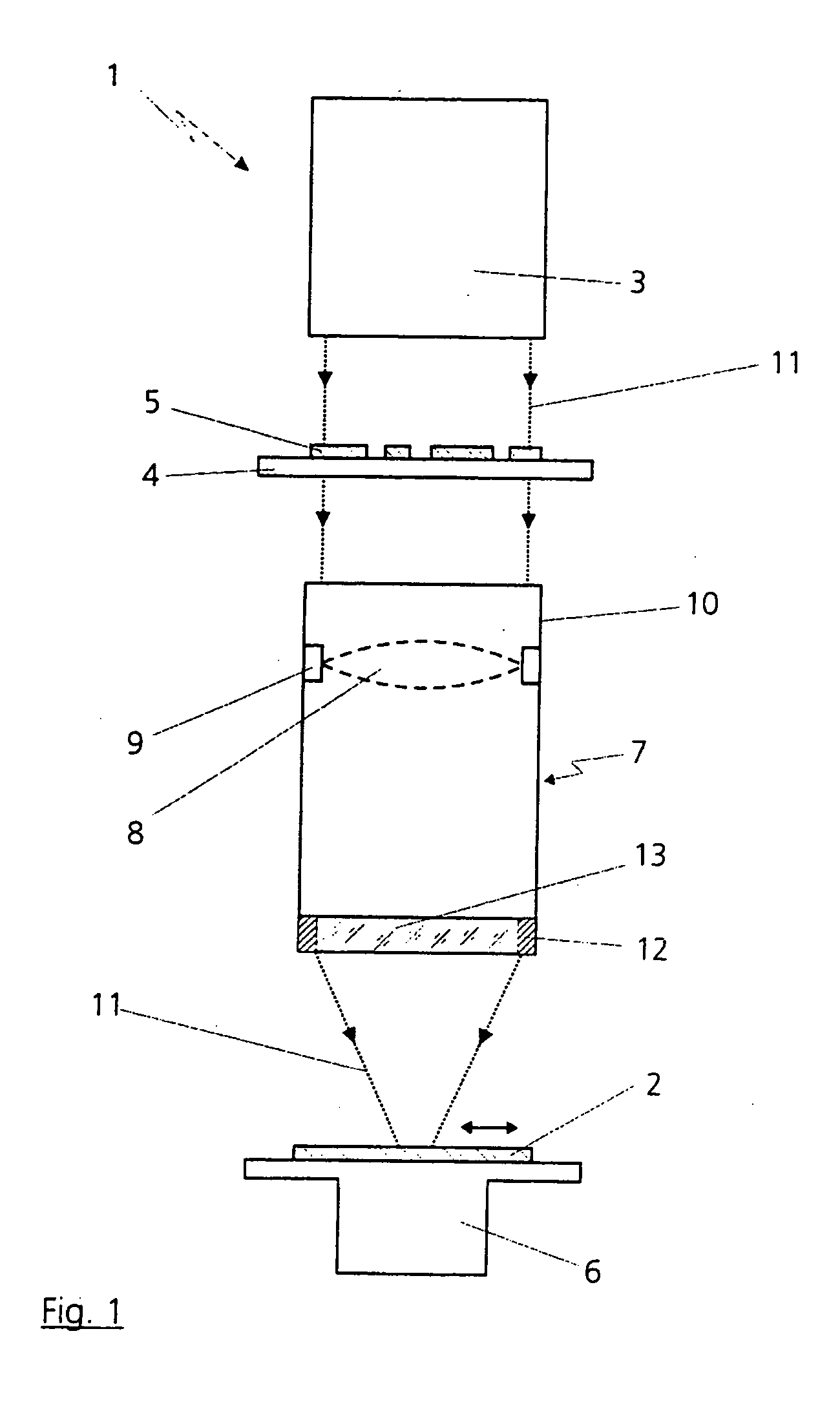
[0033]FIG. 1 illustrates a projection exposure system 1 for microlithography. This is used to expose structures on a substrate coated with photosensitive materials, which generally predominantly consists of silicon and is designated a wafer 2, for the production of semiconductor components, such as computer chips.
[0034] The projection exposure system 1 in this case substantially comprises an illuminating device 3, a device 4 for holding and exactly positioning a mask provided with a grid-like structure, what is known as a reticle 5, by which the subsequent structures on the wafer 2 are determined, a device 6 for holding, moving and exactly positioning just this wafer 2, and an imaging device, specifically a projection objective 7 having a plurality of optical elements, such as lenses 8, which are mounted via a mount 9 in an objective housing 10 of the projection objective 7.
[0035] The fundamental functional principle in this case provides for the structures introduced into the ret...
PUM
 Abstract
Description
Claims
Application Information


