

Semiconductor laser device and method for fabricating the same
- Summary
- Abstract
- Description
- Claims
- Application Information
AI Technical Summary
Benefits of technology
Problems solved by technology
Method used
Image

Examples
Embodiment Construction
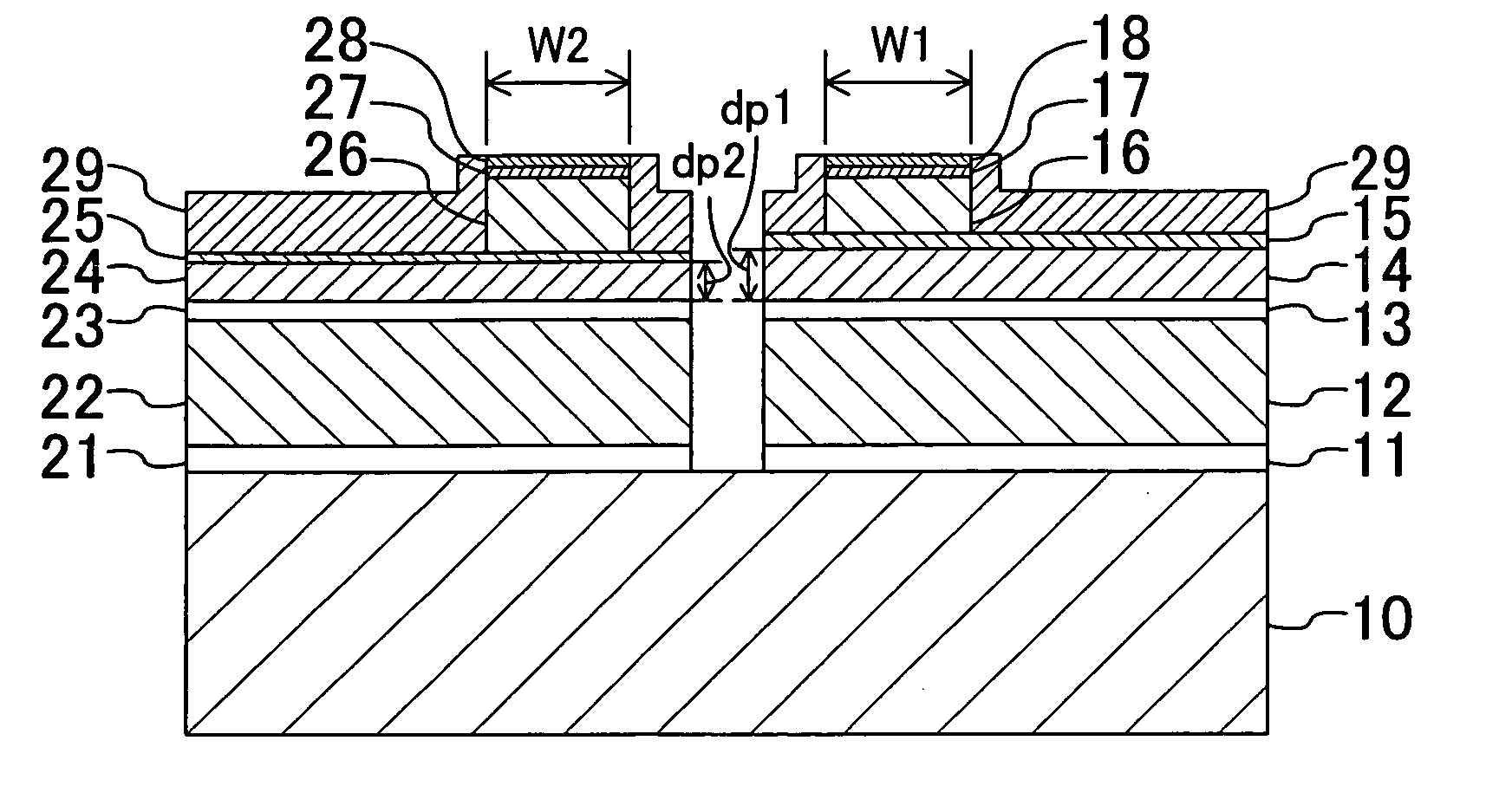
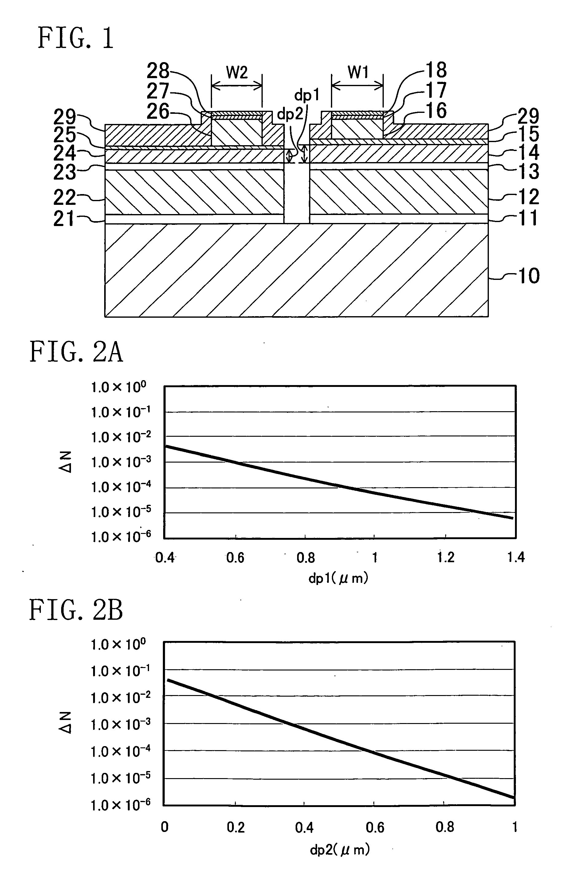
[0063] Hereinafter, a semiconductor laser device and a method for fabricating the device according an embodiment of the present invention will be described with reference to the drawings.
[0064]FIG. 1 is a cross-sectional view schematically illustrating a structure of a semiconductor laser device according to an embodiment of the present invention. In the structure illustrated in FIG. 1, a red laser and an infrared laser are integrated on an n-type GaAs substrate 10 whose principal plane is inclined with respect to the (100) plane toward the [011] direction at 10°, for example.
[0065] First, a structure of the infrared laser will be described. In the infrared laser, an n-type GaAs buffer layer 11 (with a thickness of 0.5 μm), an n-type (Al0.7Ga0.3)0.51In0.49P lower cladding layer 12 (with a thickness of 2.0 μm), an AlGaAs-based active layer 13 (with a thickness of 200 Å) having a quantum well structure and containing GaAs, a p-type (Al0.7Ga0.3)0.51In0.49P first upper cladding layer ...
PUM
 Abstract
Description
Claims
Application Information