Photonic integrated circuit device and elements thereof

a technology of integrated circuits and components, applied in the field of photonic integrated circuits, can solve the problems of limited communication capacity of chips, boards, modules, subsystems of chips, etc., and achieve the effects of improving functionality, structure and capabilities, and configurability of pic devices

Inactive Publication Date: 2006-07-20
HANDELMAN DORON
View PDF83 Cites 22 Cited by
  • Summary
  • Abstract
  • Description
  • Claims
  • Application Information

AI Technical Summary

Benefits of technology

[0033] The present invention, in preferred embodiments thereof, seeks to provide photonic integrated circuit (PIC) devices with improved functionality, structure and capabilities, particularly, but not only, with respect to architecture of the PIC devices, configurability of the PIC devices, communication...

Problems solved by technology

Increase of communication capacity within chips, boards, modules, and subsystems of chips is limited to...

Method used


Image

  • Photonic integrated circuit device and elements thereof
  • Photonic integrated circuit device and elements thereof
  • Photonic integrated circuit device and elements thereof

Examples


Embodiment Construction

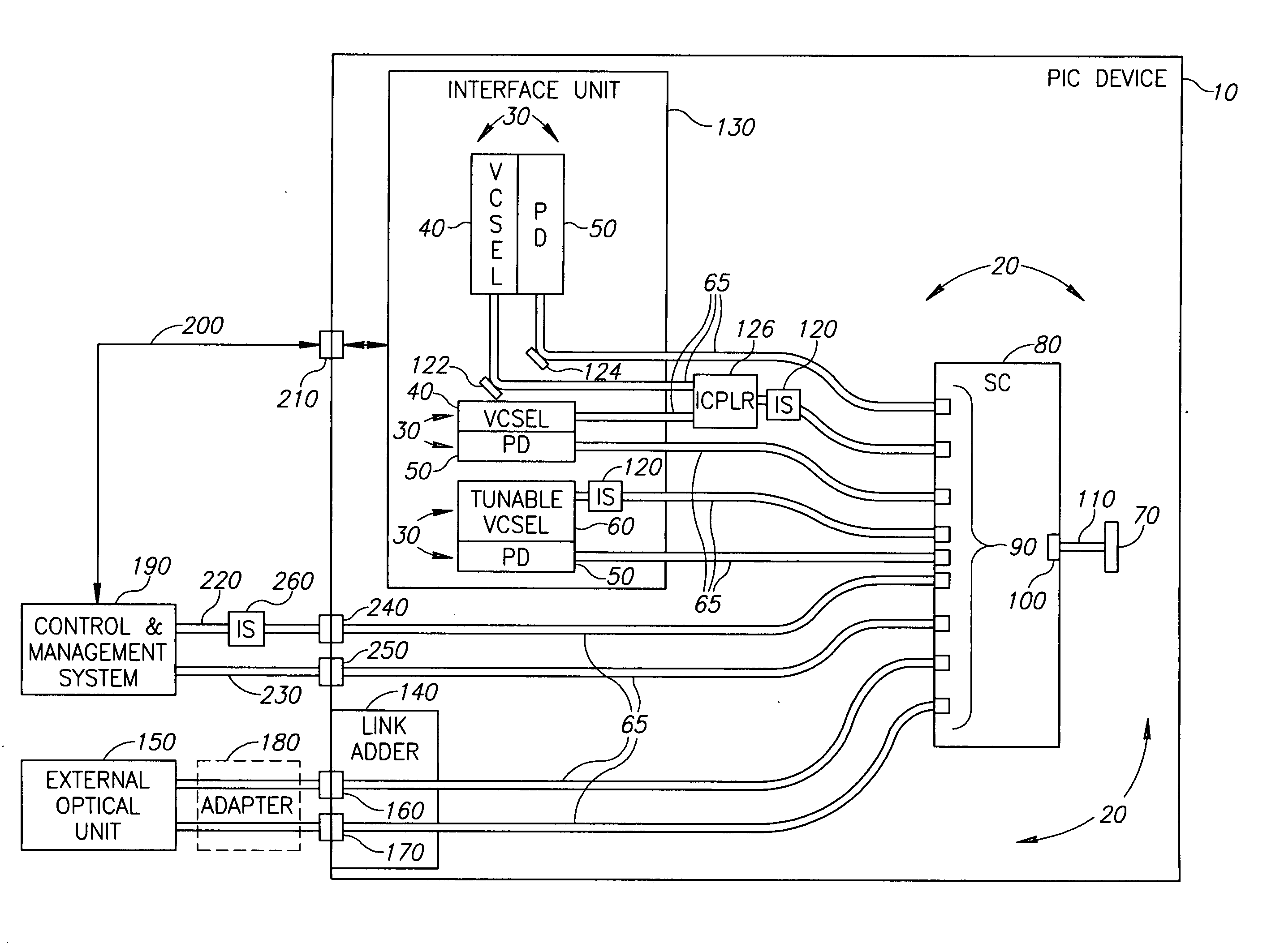
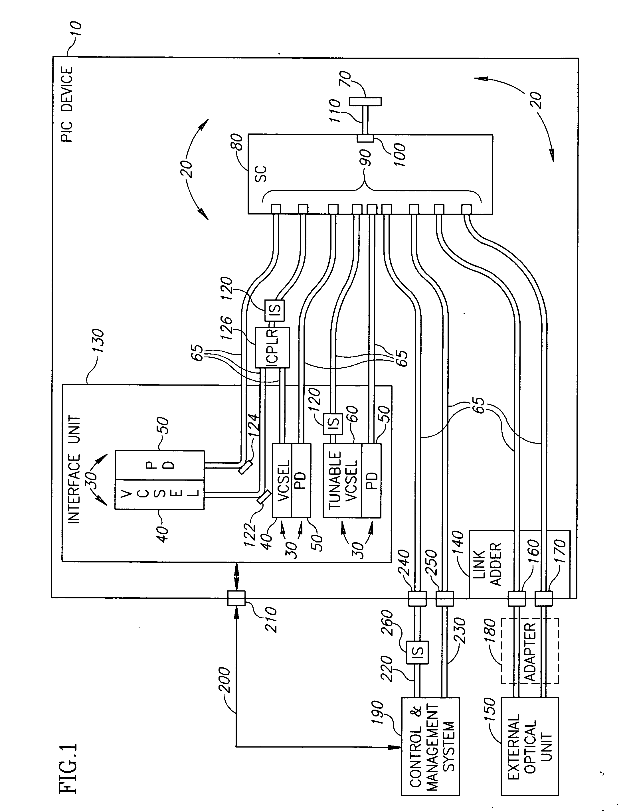
[0104] The present invention, in preferred embodiments thereof, seeks to provide photonic integrated circuit (PIC) devices with improved functionality, structure and capabilities, particularly, but not only, with respect to architecture of the PIC devices, configurability of the PIC devices, communication between optical transceivers comprised in or associated with the PIC devices, protection and restoration of communication between optical transceivers comprised in or associated with the PIC devices, and operability of the PIC devices and of optical transceivers comprised in or associated with the PIC devices. Such PIC devices may, for example, be useful as building blocks or entire systems in various applications including, for example which is not meant to be limiting, the following applications: optical switching and routing applications; applications involving chip-to-chip communication; applications involving linecard-to-linecard communication and optical backplane application...


PUM


Abstract

A photonic integrated circuit (PIC) device is described. The PIC device includes a set of optical transceivers including optical transmitters and optical receivers, and an embedded optical interconnect mesh operatively associated with the set of optical transceivers and structured to enable at least one of the following network architectures: a star network architecture, a bus/broadcast network architecture, and a ring network architecture. Related apparatus and methods are also described.

Description

FIELD OF THE INVENTION [0001] The present invention generally relates to photonic integrated circuit (PIC) devices with optical interconnects and to elements thereof. BACKGROUND OF THE INVENTION [0002] Increase of communication capacity within chips, boards, modules, and subsystems of chips is limited today due to the electrical interconnects that are used in the chips, boards, modules, and subsystems of chips. Optical interconnects are considered as enabling better performance than electrical interconnects, for example in terms of bandwidth and susceptibility to electromagnetic noise, and therefore photonic integrated circuit (PIC) devices that use optical interconnects have been developed. [0003] PIC devices and optical interconnects for optical backplanes and chip-to-chip communication are described in the following publications: [0004] Published US Patent application US2004 / 0067006 A1 of Welch et al, which describes transmitter photonic integrated circuit (TXPIC) chips; [0005] a...

Claims


Application Information

Patent Timeline
IPC IPC(8): G02B6/12
CPCG02B6/4246G02B6/43
Inventor HANDELMAN, DORON
Owner HANDELMAN DORON
Why Eureka
Try Eureka