Single layer type electrophotographic photoconductor and image forming device

an electrophotographic photoconductor and single layer technology, applied in the field of single layer electrophotographic photoconductor and image forming device, can solve the problems of black spots and black stripes on the image of the organic single layer type photoconductor, and achieve the effects of reducing the generation of black spots, excellent sensitivity, and effective prevention of silica and paper powder adhesion

Active Publication Date: 2006-07-20
KYOCERA DOCUMENT SOLUTIONS INC
View PDF2 Cites 10 Cited by
  • Summary
  • Abstract
  • Description
  • Claims
  • Application Information

AI Technical Summary

Benefits of technology

[0029] That is, according to the single layer type electrophotographic photoconductor of the present invention, the photoconductor contains the water-repellant polycarbonate resin and the contact angle of the pure water with respect to the photoconductive layer is set to the given value or more and hence, the adhesion of silica and paper powders is effectively prevented whereby the photoconductor exhibits the excellent sensitivity characteristic even after a long-time use thereof thus effectively decreasing the generation of black spots.
[0030] Further, according to the single layer type electrophotographic photoconductor of the present invention, by setting the contact angle of the pure water with respect to the water-repellant polycarbonate resin to the given value or more, it is possible to easily adjust the contact angle of the pure water with respect to the photoconductive layer and hence, the adhesion of silica and paper powders is more effectively prevented thus effectively decreasing the generation of black spots.
[0031] Further, according to the single layer type electrophotographic photoconductor of the present invention, the photoconductor contains the polycarbonate resin having the siloxane structure as the water-repellant polycarbonate resin and hence, it is possible to easily adjust the contact angle of the pure water with respect to the photoconductive layer and, at the same time, the more excellent durability can be obtained.
[0032] Further, according to the single layer type electrophotographic photoconductor of the present invention, by setting the content ratio of the polycarbonate resin having the siloxane structure to a value which falls within a given range, the contact angle of the photoconductive layer can be easily adjusted and hence, the more excellent durability can be obtained.
[0033] Further, according to the single layer type electrophotographic photoconductor of the present invention, since the polycarbonate resin having the siloxane structure exists non-uniformly in the surface of the photoconductive layer, it is possible to obtain the excellent filming property and durability even when the content ratio of the polycarbonate resin is relatively small.
[0034] Further, according to the single layer type electrophotographic photoconductor of the present invention, the resin dispersion film of the hole transporting agent has the given contact angle and hence, coupled with a water-repellant function of the water-repellant polycarbonate resin, the adhesion of silica and paper powders can be prevented more effectively whereby the generation of black spots can be effectively decreased.

Problems solved by technology

Since the transferring sheet is charged in a negative polarity, paper powders which are charged in the negative polarity is easily adhered to the photoconductor charged in the positive polarity whereby there frequently arises a drawback that the organic single layer type photoconductor generates black spots and black stripes on the image.

Method used


Image

  • Single layer type electrophotographic photoconductor and image forming device
  • Single layer type electrophotographic photoconductor and image forming device
  • Single layer type electrophotographic photoconductor and image forming device

Examples


first embodiment

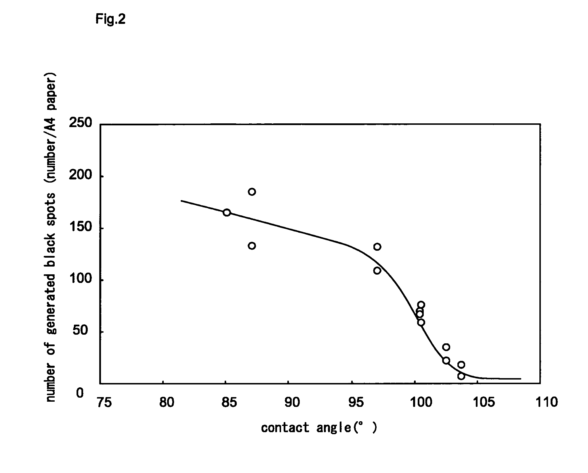
[0048] The first embodiment is directed to a single layer type electrophotographic photoconductor which includes a photoconductive layer containing a binding resin, a hole transporting agent and an electron generating agent, wherein the photoconductor contains a water-repellant polycarbonate resin as the binding resin, and a contact angle of pure water with respect to the photoconductive layer is set to 100° or more.

1. Basic Constitution

(1) Structure

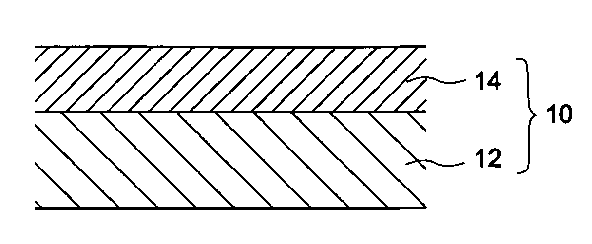
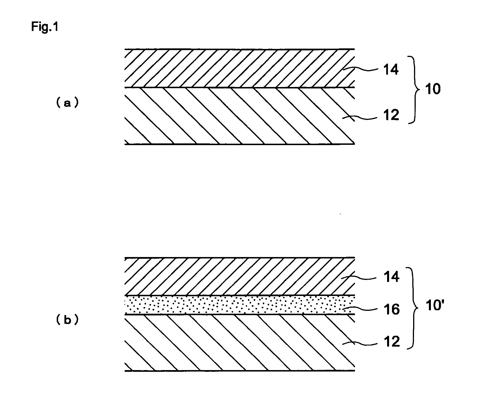
[0049] As shown in FIG. 1(a), a single layer type photoconductor 10 is configured by having a single photoconductive layer 14 on a base body 12.

[0050] The photoconductive layer contains a binding resin, a hole transporting agent and a charge generating agent. Further, the photoconductive layer also contains an electron transporting agent, a leveling agent or an additive such as silyl-group containing compound or the like when necessary.

[0051] The obtained single layer type photoconductor contains a water-repellant polycarbonate re...

second embodiment

[0137] Second embodiment is directed to an image forming device which is characterized in that the image forming device includes the single layer type electrophotographic photoconductor (hereinafter, occasionally simply referred to as a photoconductor) of the first embodiment, arranges a charging step, an exposure step, an developing step and a transferring step respectively around the electrophotographic photoconductor, and performs the image forming.

[0138] In carrying out the image forming method of the second embodiment, a copying machine 30 which constitutes an image forming device as shown in FIG. 4 is favorably used. The copying machine 30 includes an image forming unit 31, a paper ejection unit 32, an image reading unit 33 and an original feeding unit 34. Further, an image forming portion 31a and a paper feeding portion 31b are further provided to the image forming unit 31. Further, in the example illustrated in the drawing, the paper feeding unit 34 includes a paper storing...

example

Example 1

1. Preparation of Electrophotographic Photoconductor

[0152] 4 parts by weight of X type non-metal phthalocyanine (CGM-A) represented by formula (30) as the charge generating agent, 50 parts by weight of a stilbene derivative (HTM-A) represented by formula (10) as a hole transporting agent, 30 parts by weight of a naphthoquinone derivative (ETM-A) represented by formula (22) as an electron transporting agent, 100 parts by weight of a polycarbonate resin (Resin-A) represented by formula (6) having a viscosity average molecular weight of 20,000 as a binding resin, and 800 parts by weight of tetrahydrofuran as a solvent are filled in a vessel.

[0153] Next, the contents of the vessel are mixed and dispersed using a ball mill for 50 hours thus preparing a coating liquid to be applied to the single layer type photoconductive layer. The prepared coating liquid is applied to a base body (an aluminum stock tube) having a diameter of 30 mm using a dip coating method and is dried wit...


PUM

PropertyMeasurementUnit
temperatureaaaaaaaaaa
diameteraaaaaaaaaa
rotational speedaaaaaaaaaa

Abstract

The present invention provides a single layer type electrophotographic photoconductor which exhibits the small number of generated black spots in a formed image and exhibits the excellent sensitivity characteristic even when the photoconductor is used for a long time or a photoconductor drum is rotated at a high speed and an image display device which includes the single layer type electrophotographic photoconductor. In the single layer type electrophotographic photoconductor which includes a photoconductive layer containing a binding resin, a hole transporting agent and an charge generating agent, the photoconductor contains a water-repellant polycarbonate resin as the binding resin, and a contact angle of pure water (measured temperature: 25° C.) with respect to the photoconductive layer is set to 100° or more.

Description

TECHNICAL FIELD [0001] The present invention relates to a single layer type electrophotographic photoconductor and an image forming device, and more particularly, to a single layer type electrophotographic photoconductor which generates few black spots even when the single layer type electrophotographic photoconductor is used for a long time and an image forming device having such a single layer type electrophotographic photoconductor. BACKGROUND OF THE INVENTION [0002] Conventionally, as an electrophotographic photoconductor provided to an image forming device and the like, an organic photoconductor (OPC) which contains a binding resin (a binder resin), a charge generating agent, and a charge transporting agent (a hole transporting agent, an electron transporting agent) and the like has been used. Such an organic photoconductor has, compared to a conventional inorganic photoconductor, advantages such as the easy manufacturing thereof, the high degree of freedom in structural design...

Claims


Application Information

Patent Timeline
Patent Type & Authority Applications(United States)
IPC IPC(8): G03G5/05
CPCG03G5/0517G03G5/0564G03G5/0578G03G5/0592G03G5/0609G03G5/0614G03G5/0651G03G5/0696G03G5/102G03G5/06144G03G5/061443G03G5/06147G03G5/061473
Inventor KUBOSHIMA, DAISUKEHAMASAKI, KAZUNARINAKAI, NORIO
Owner KYOCERA DOCUMENT SOLUTIONS INC
Why Eureka
Try Eureka