MOS transistor with elevated source/drain structure

a technology of source/drain structure and mos transistor, which is applied in the field of metaloxide semiconductor (mos) transistor with an elevated source/drain structure, can solve the problems of reducing the punch-through characteristics between the source electrode, ldd structure is limited in use, and the extent to which the junction depth can be reduced

Active Publication Date: 2006-07-27
SAMSUNG ELECTRONICS CO LTD
View PDF13 Cites 43 Cited by
  • Summary
  • Abstract
  • Description
  • Claims
  • Application Information

AI Technical Summary

Benefits of technology

[0008] In a metal-oxide semiconductor (MOS) transistor with an elevated source / drain structure and in a method of fabricating the MOS transistor with the elevated source / drain structure using a selective epitaxy growth (SEG) process, a source / drain extension junction is formed after an epi-layer is formed, thereby preventing degradation of the source / drain junction region. In addition, the source / drain extension junction is partially overlapped by a lower portion of the gate layer, since two gate spacers are formed and two elevated source / drain layers are formed in accordance with the SEG process. This mitigates the short channel effect and reduces sheet resistance in the source / drain layers and in the gate layer.

Problems solved by technology

This, in turn, causes an undesirable effect, referred to as the “short-channel” effect, which degrades the punch-through characteristics between a source electrode and a drain electrode of the FET.
However, such an LDD structure is limited in use, since it can be applied to only a semiconductor element with a gate line width of 0.35 μm or larger to suppress the short channel effect, and cannot be applied to a semiconductor element with a gate line width of 0.35 μm or less.
This is because there is a limit to the extent to which the depth of the junction can be reduced, and thus formation of a junction in the LDD structure is impractical or impossible.

Method used


Image

  • MOS transistor with elevated source/drain structure
  • MOS transistor with elevated source/drain structure
  • MOS transistor with elevated source/drain structure

Examples


Embodiment Construction

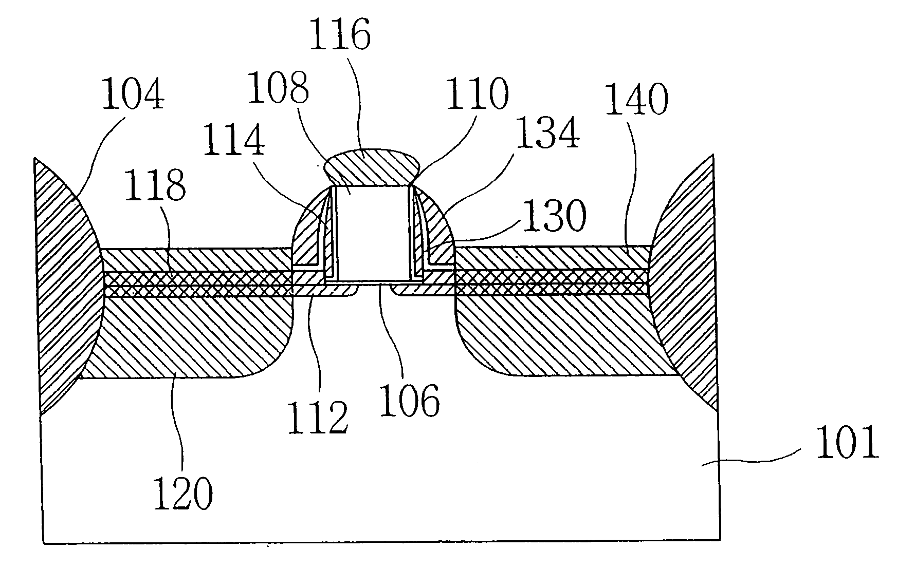
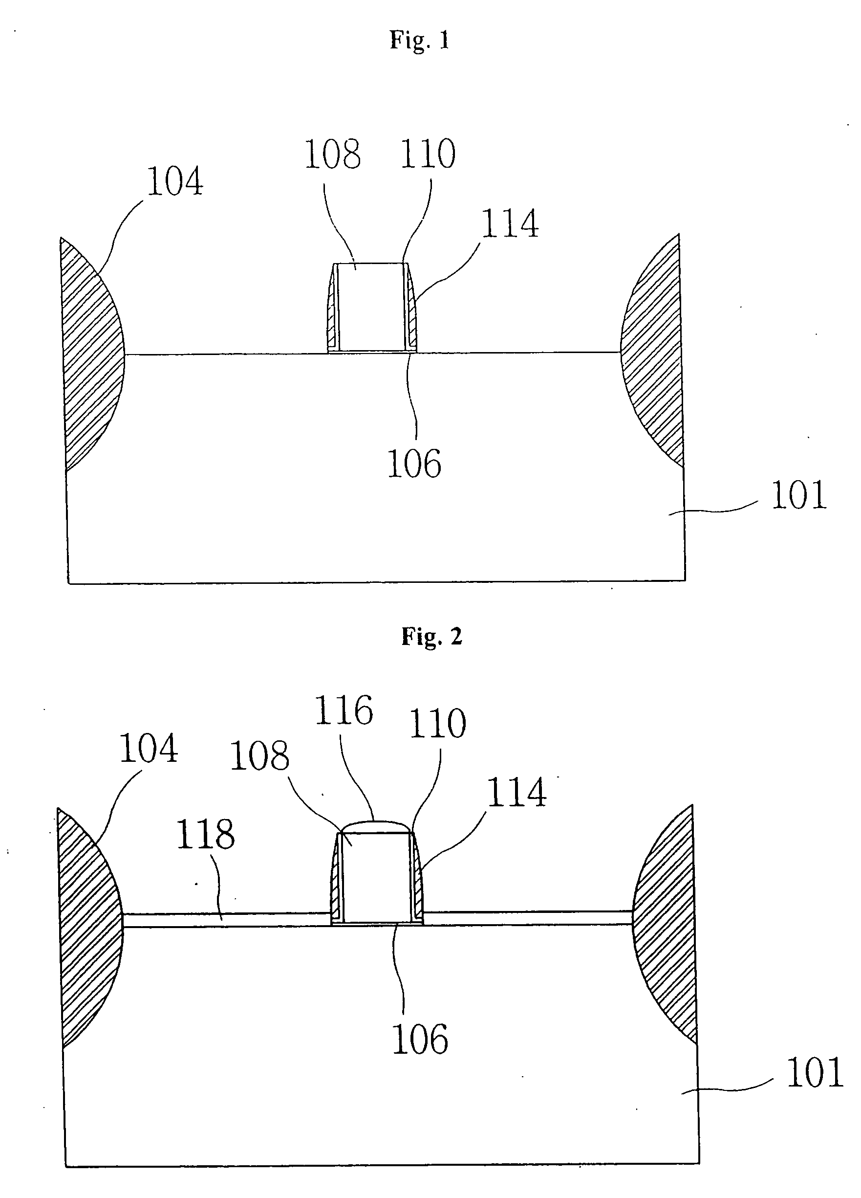
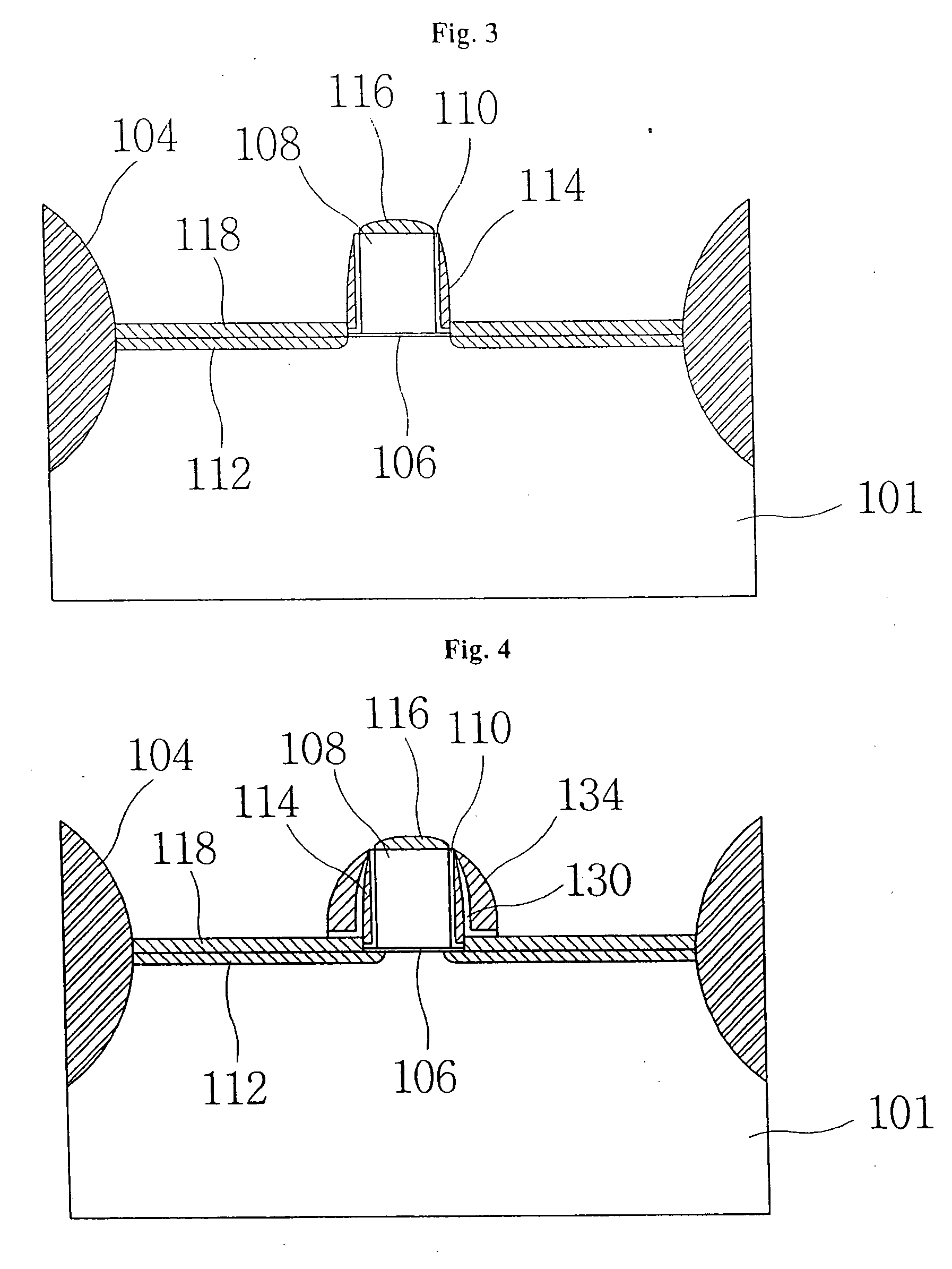
[0027] FIGS. 1 to 6 are sectional views illustrating the fabrication of an MOS transistor with an elevated source / drain structure according to the present invention.

[0028] With reference to FIG. 1, device separators 104, or isolation structures, are formed on a semiconductor substrate 101 to define an active area, or active region, between the separators 104. Preferably, the semiconductor substrate 101 is composed of silicon. The device separators may be formed, for example, by any of the well-known techniques including the formation of field oxide structures 104 according to the local oxidation of silicon (LOCOS) process, and the shallow trench isolation (STI) method.

[0029] A gate dielectric 106 is formed on the active region of the semiconductor substrate 101, for example, by a deposit of a material selected from the group consisting of SiO2, SiON, SiN, Al2O3, and mixtures thereof. In one embodiment, the resulting gate dielectric 106 thus formed is 20 to 100 Å in thickness.

[003...


PUM


Abstract

In a metal-oxide semiconductor (MOS) transistor with an elevated source / drain structure and in a method of fabricating the MOS transistor with the elevated source / drain structure using a selective epitaxy growth (SEG) process, a source / drain extension junction is formed after an epi-layer is formed, thereby preventing degradation of the source / drain junction region. In addition, the source / drain extension junction is partially overlapped by a lower portion of the gate layer, since two gate spacers are formed and two elevated source / drain layers are formed in accordance with the SEG process. This mitigates the short channel effect and reduces sheet resistance in the source / drain layers and the gate layer.

Description

RELATED APPLICATIONS [0001] This application is a divisional of U.S. patent application Ser. No. 10 / 823,420, filed on Apr. 13, 2004, which claims priority under 35 U.S.C. §119 to Korean Patent Application No. 10-2003-0030614, filed May 14, 2003, the contents of which are incorporated herein by reference, in their entirety.BACKGROUND OF THE INVENTION [0002] 1. Field of the Invention [0003] The present invention pertains, in general, to a semiconductor element and a method of fabricating the same and, more particularly, to a metal-oxide semiconductor (MOS) transistor with an elevated source / drain structure and a method of fabricating the same, using a selective epitaxial growth (SEG) process. [0004] 2. Description of the Related Art [0005] As well-known to those skilled in the art, Field Effect Transistors (FET) have been gradually scaled down in size in accordance with the recent trend toward small-sized, lightweight, and slim electronic devices. However, as a result of the downsizin...

Claims


Application Information

Patent Timeline
Patent Type & Authority Applications(United States)
IPC IPC(8): H01L31/109H01L21/336H01L29/78
CPCH01L29/42376H01L29/66477H01L29/665H01L29/6656H01L29/66628H01L29/7834H01L21/18
Inventor LEE, SEUNG-HWANPARK, MOON-HANRHEE, HWA-SUNGLEE, HOYOO, JAE-YOON
Owner SAMSUNG ELECTRONICS CO LTD
Why Eureka
Try Eureka