
Magnetic field sensing device and a fabricating method of the same

Active Publication Date: 2006-07-27
SAMSUNG ELECTRONICS CO LTD
View PDF7 Cites 5 Cited by
  • Summary
  • Abstract
  • Description
  • Claims
  • Application Information

AI Technical Summary

Benefits of technology

[0017] It is, therefore, an object of the present invention to provide a magnetic field sensing device and a fabrication method of the same, for facilitating the planarization of a substrate in every fabrication process.
[0018] It is another object of the present invention to provide a magnetic field sensing device and a fabrication method of the same, which features an easy formation of a contact hole and a reduced inferiority rate in the formation of the contact hole by reducing the thickness of an insulating film.
[0019] It is still another object of the present invention to provide a magnetic field sensing device and a fabrication method of the same, for reducing a stepped portion of a second insulating film and thereby, facilitating the formation of a second coil.
[0021] It is yet another object of the present invention to provide a magnetic field sensing device and a fabrication method of the same, for increasing the thickness of a magnetic substance and thereby, facilitating the fabrication process.

Problems solved by technology

Also, it has a great impact on the degree of planarization of a substrate in every process, difficulty of the fabrication process, defective proportion, and performance of the magnetic field sensing device.
This consequently puts impediments in the way of fabricating small-sized magnetic field sensing devices.
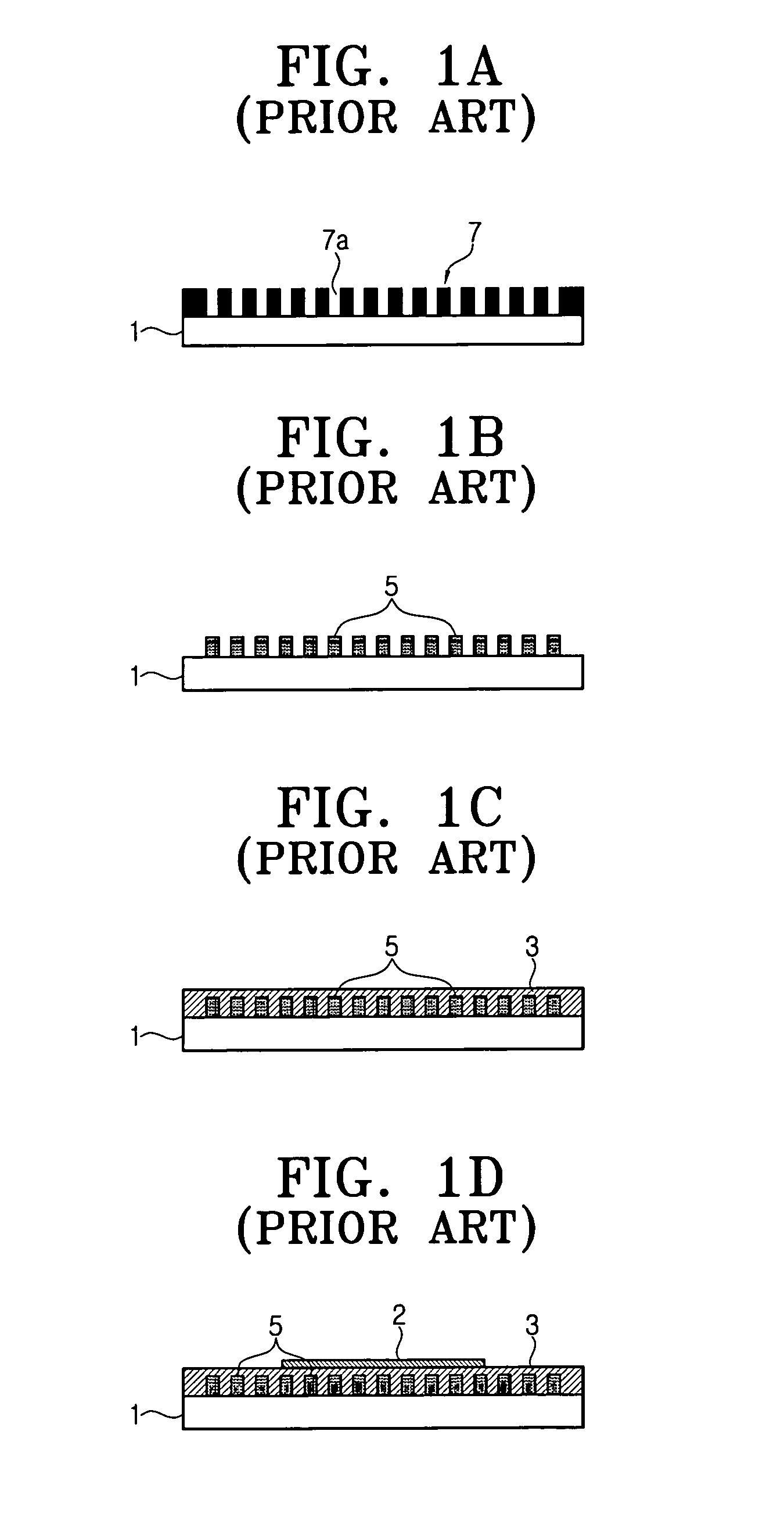
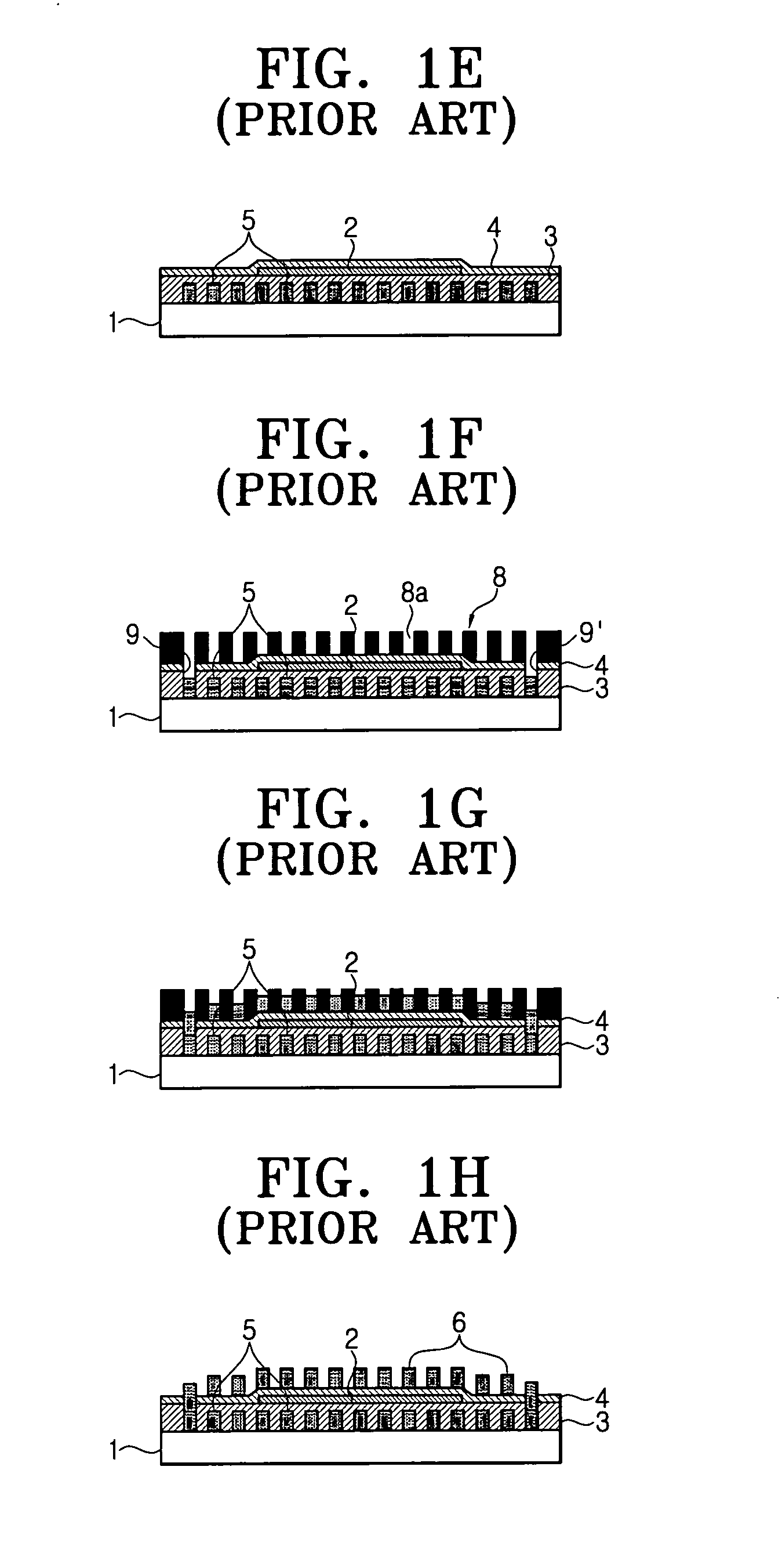
However, if the thickness of the insulating films 3 and 4 is increased, not only the entire thickness of the device is also increased, but also the process (i.e., etching) for forming the through holes 9 and 9′ connecting the first coil 5 and the second coil 6 becomes very difficult, often resulting in a high inferiority rate.

Method used


Image

  • Magnetic field sensing device and a fabricating method of the same
  • Magnetic field sensing device and a fabricating method of the same
  • Magnetic field sensing device and a fabricating method of the same

Examples


Embodiment Construction

[0032] An exemplary embodiment of the present invention will be described herein below with reference to the accompanying drawings.

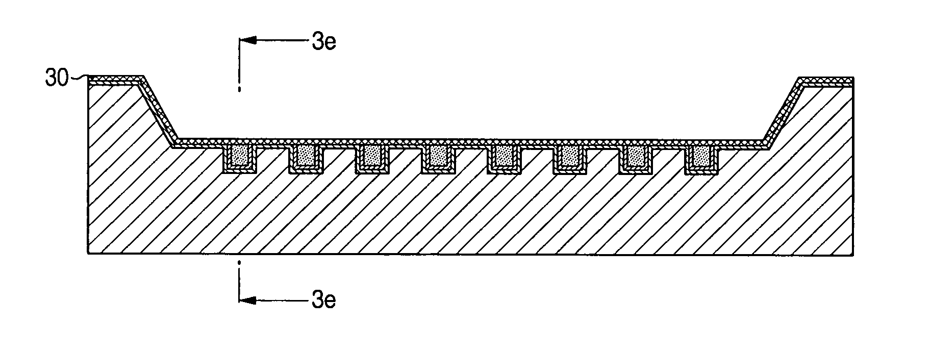
[0033]FIGS. 2A to 2I are cross-sectional views of a magnetic field sensing device and a fabrication method of the same, according to an exemplary embodiment of the present invention, and FIGS. 3A to 3I are cross-sectional views of FIGS. 2A to 2I, respectively.

[0034] As shown in FIG. 2I and FIG. 3I, the magnetic field sensing device of an exemplary embodiment of the invention includes a substrate 10, a magnetic substance 20 formed on the substrate 10, a plurality of wires (51, 52 . . . ) (61, 62 . . . ) (hereinafter, called collectively 51, 61), a first and a second coil 50, 60 provided to the lower and the upper portion of the magnetic substance 20, respectively, and a first and a second insulating film 30, 40 interposed between the first and second coils 50 and 60 and the magnetic substance 20 for insulating the magnetic substance 20 from the first an...


PUM


Abstract

A magnetic field sensing device and a fabrication method of the same featuring an easy planarization profess for a substrate and a simplified procedure by the benefit of a slim planarizing substance. The magnetic field sensing device includes a substrate with a well of a predetermined depth and a plurality of grooves being formed thereon and a magnetic substance formed on an inner surface of the well to be located on an upper portion of the grooves. A first coil is formed in the grooves, a second coil is formed on an upper portion of the magnetic substance and is electrically connected to the first coil and insulating films are interposed between the first and the second coil and the magnetic substance for insulating the first and the second coil from the magnetic substance.

Description

CROSS-REFERENCE TO RELATED APPLICATIONS [0001] This application claims benefit under 35 U.S.C. § 119 from Korean Patent Application No. 2005-06772, filed on Jan. 25, 2005, the entire content of which is incorporated herein by reference. BACKGROUND OF THE INVENTION [0002] 1. Field of the Invention [0003] The present invention relates to a micro magnetic field sensing device and a fabrication method of the same. [0004] 2. Description of the Related Art [0005] A magnetic sensor composed of a magnetic substance and coils is highly sensitive to very small applied magnetic fields. In general, a magnetic sensor is fabricated by winding coils around a soft magnetic core, and requires an electronic circuit for generating a magnetic field proportional to a magnetic field measurement. A magnetic field sensing device for the magnetic sensor can be realized by a thin-film soft magnetic core and planar thin film coils. [0006]FIGS. 1A to 1H are diagrams for explaining a related art magnetic field ...

Claims


Application Information

Patent Timeline
IPC IPC(8): G11B5/147G11B5/33
CPCG01R33/05B62D49/02B60Y2200/221B60Y2304/05
Inventor NA, KYUNG-WON
Owner SAMSUNG ELECTRONICS CO LTD
Learn More