

PLL circuit and program for same
- Summary
- Abstract
- Description
- Claims
- Application Information
AI Technical Summary
Benefits of technology
Problems solved by technology
Method used
Image

Examples
first embodiment
of the Present Invention
[0116] The following explanation regards the details of the configuration of the first embodiment of the present invention with reference to the accompanying figures.
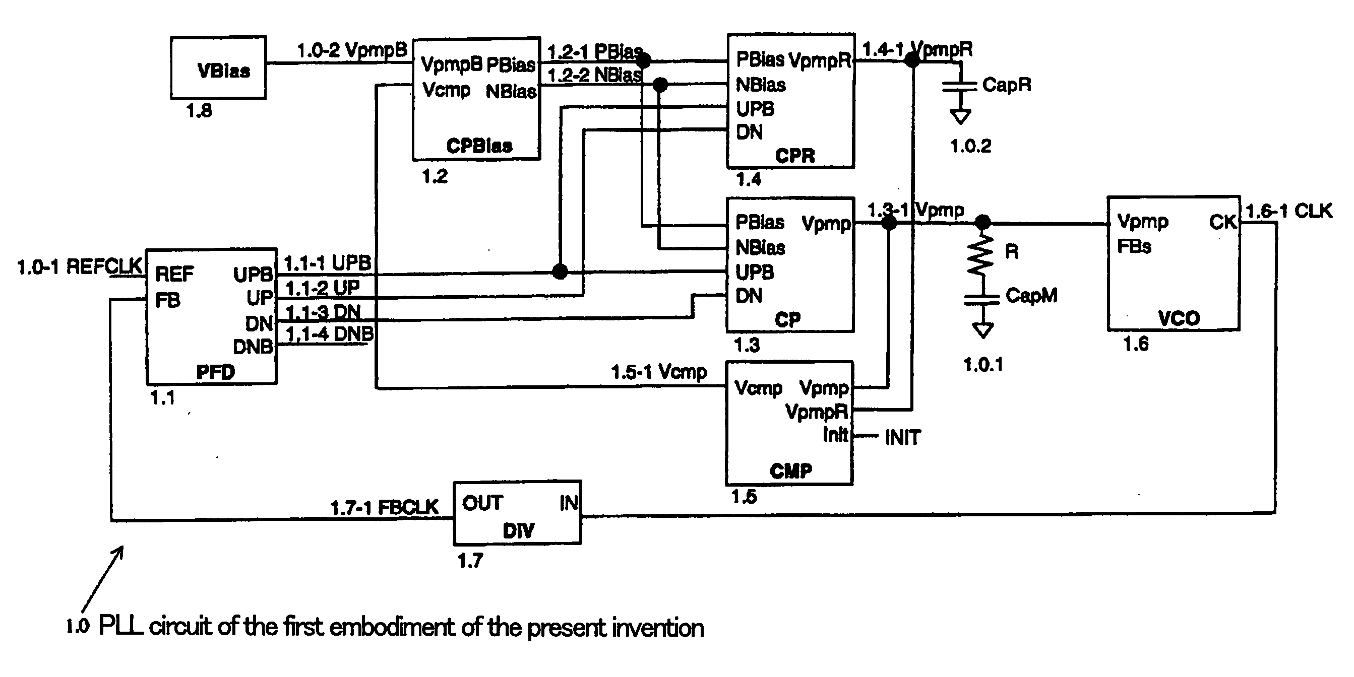
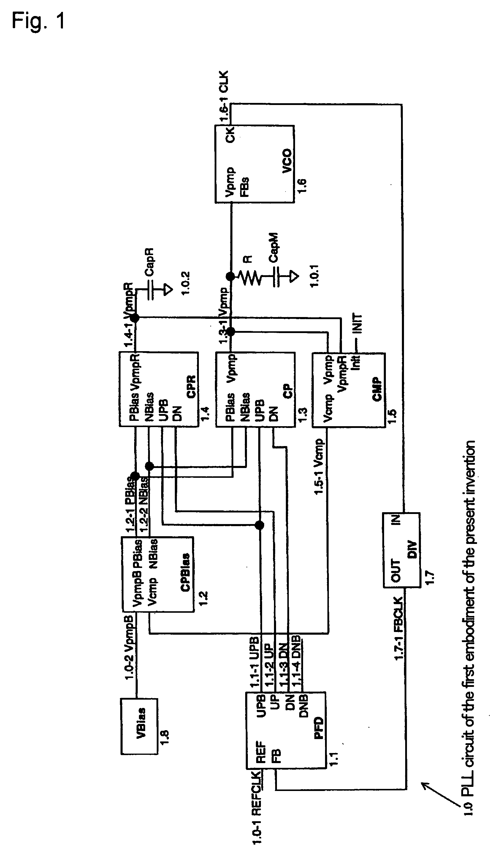
[0117]FIG. 1 is a block diagram showing the overall configuration of PLL circuit 1.0 of the first embodiment of the present invention. PLL circuit 1.0 of the first embodiment of the present invention is composed of:
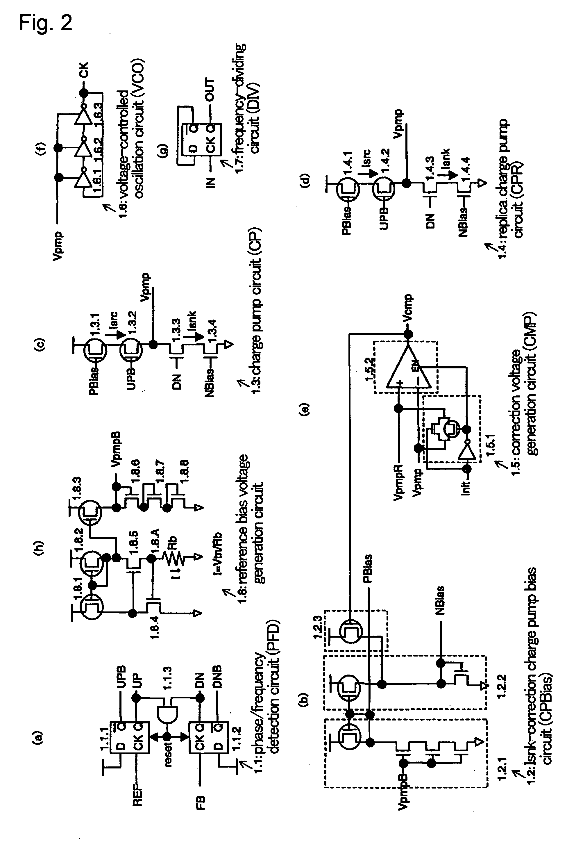
[0118] Phase / frequency detection circuit 1.1 is further composed of: data flip-flop circuits (D-F / F) 1.1.1 and 1.1.2, and reset circuit 1.1.3; Isnk-correction charge pump bias circuit 1.2 is further composed of bias current generation circuit 1.2.1, bias current mirror circuit 1.2.2, and bias current correction circuit 1.2.3; charge pump circuit 1.3 is further composed of Isrc-supply constant-current PMOS 1.3.1, Isrc switch PMOS 1.3.2, Isnk switch NMOS 1.3.3, and Isnk-supply constant-current NMOS 1.3.4; replica charge pump circuit 1.4 is further composed of Isrc-supply constant-curre...
second embodiment
of the Present Invention
[0134] The following explanation regards the details of the second embodiment of the present invention with reference to the accompanying figures.
[0135]FIG. 6 is a block diagram showing the overall configuration of PLL circuit 2.0 of the second embodiment of the present invention. Although no changes are made to the block configuration of the first embodiment, the circuit configuration of Isnk-correction charge pump bias circuit 1.2 is changed to Isrc-correction charge pump bias circuit 2.2, and the effect that was obtained by correcting Isnk in the first embodiment is obtained by correcting Isrc in the second embodiment.
[0136]FIG. 7 shows Isrc-correction charge pump bias circuit 2.2. This Isrc-correction charge pump bias circuit 2.2 is composed of: bias current generation circuit 2.2.1 for obtaining a desired Isrc and Isnk; bias current mirror circuit 2.2.2 for converting the bias current to Isnk bias voltage NBias that determines Isnk; bias current mirror...
third embodiment
of the Present Invention
[0137] The following explanation regards the details of the third embodiment of the present invention with reference to the accompanying figures.
[0138]FIG. 8 is a block diagram showing the overall configuration of PLL circuit 3.0 of the third embodiment of the present invention. As a block configuration, this configuration is not altered from that of the first embodiment, but the circuit configuration of Isnk-correction charge pump bias circuit 1.2 is altered to Isrc / Isnk-correction charge pump bias circuit 3.2, and the effect that was obtained by correcting Isnk in the first embodiment is obtained by correcting both Isrc and Isnk in the third embodiment. FIG. 9 shows Isrc / Isnk-correction charge pump bias circuit 3.2. Isrc / Isnk-correction charge pump bias circuit 3.2 is composed of: bias current generation circuit 3.2.1 for obtaining desired Isrc and Isnk; bias current mirror circuit 3.2.2 for converting from the bias current to Isnk bias voltage NBias for d...
PUM
 Abstract
Description
Claims
Application Information