Semiconductor device and production method thereof

a technology of semiconductor devices and production methods, applied in the direction of tv systems, lighting and heating apparatus, rod connections, etc., can solve the problems of inability to realize a wafer level csp, inability to collect light, and light incident from low-melting glass, etc., to achieve the effect of inexpensive per-piece cost of a material

Inactive Publication Date: 2006-08-17
SHARP KK
View PDF19 Cites 55 Cited by
  • Summary
  • Abstract
  • Description
  • Claims
  • Application Information

AI Technical Summary

Benefits of technology

[0017] With the arrangement, it is unnecessary to use an expensive photosensitive resin material unlike a case where pattern formation is performed through photolithography. As a result, per-piece cost of a material becomes inexpensive. In conventional production methods, because the photosensitive resin material cures after formation of a pattern, a pressure of 1 through 2 MPa is necessary for combining the material to the wafer. On the other hand, in the method according to the present invention, the pattern of the spacer layer is formed through screen printing, the pattern is cured, and then the pattern of the adhesive layer is formed. Therefore, resin for the combination is not cured, and accordingly it is possible to combine the resin to the wafer with a load that is not more than 0.5 MPa.

Problems solved by technology

However, because a sensor of a light reception sensor is formed on a major part of the surface of a semiconductor, it is impossible to realize a wafer level CSP (Chip Size Package) in which a rewiring and packaging terminal is formed on the surface of the wafer.
However, there is the following problem in forming the penetrating electrode in a light reception sensor.
However, in a case of a device which increases its sensibility by forming a micro lens for collecting light on an upper part of an imaging element, the following problem may occur when the device is formed according to the aforementioned process.
The problem is such that: because there exists on the micro lens the adhesive made of transparent resin or low-melting glass used to attach the optical glass (light transmitting material), it is impossible to collect light.
As a result, light having been incident from the low-melting glass or the adhesive is not collected.
As such, imaging is difficult.
Therefore, it is difficult to evenly attach the adhesive layer to the wafer.
Therefore, there is a case where the pattern of the optical glass is not superimposed on the pattern of the wafer, with a result that problems may occur in later steps.

Method used


Image

  • Semiconductor device and production method thereof
  • Semiconductor device and production method thereof
  • Semiconductor device and production method thereof

Examples


Embodiment Construction

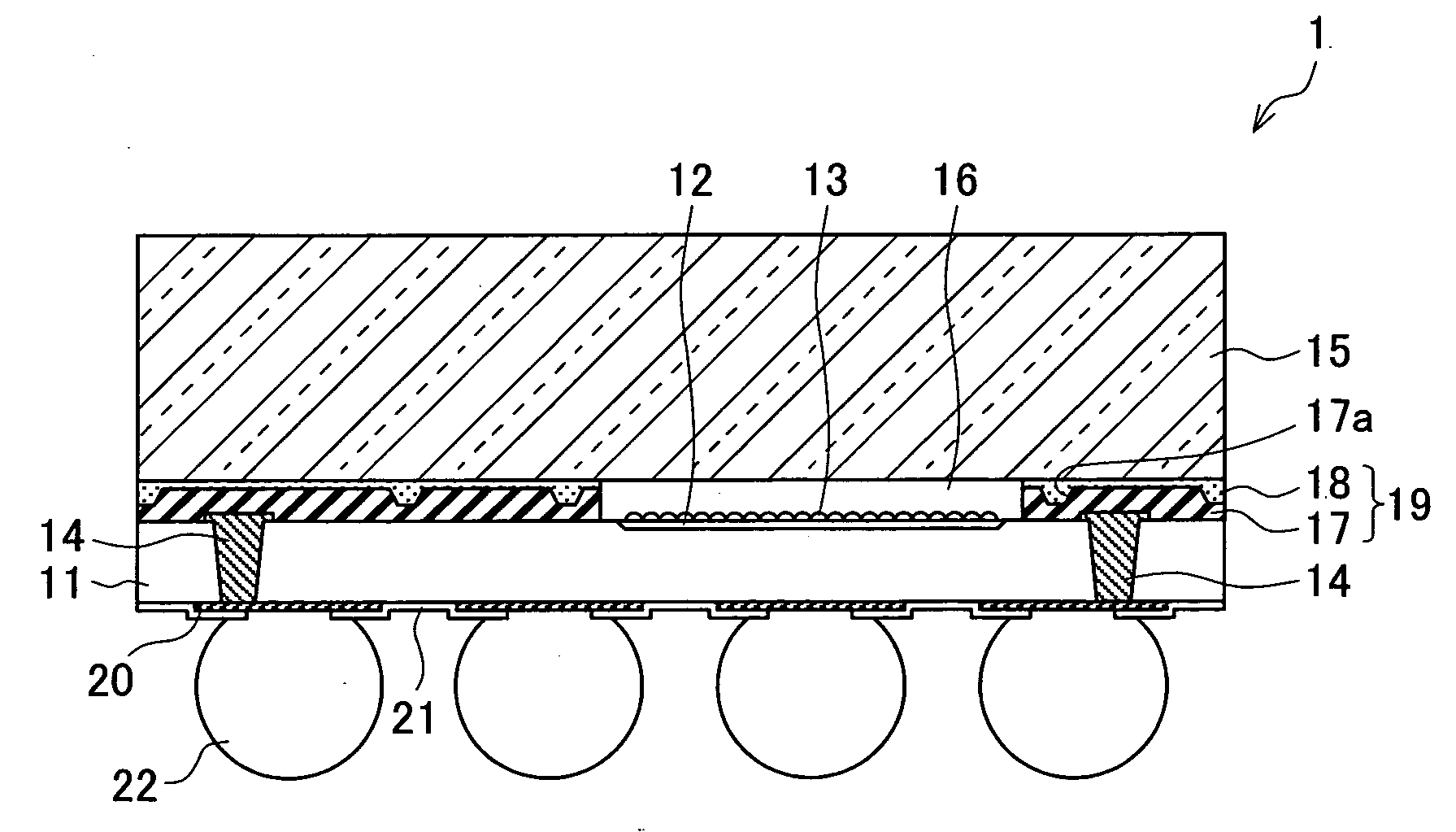
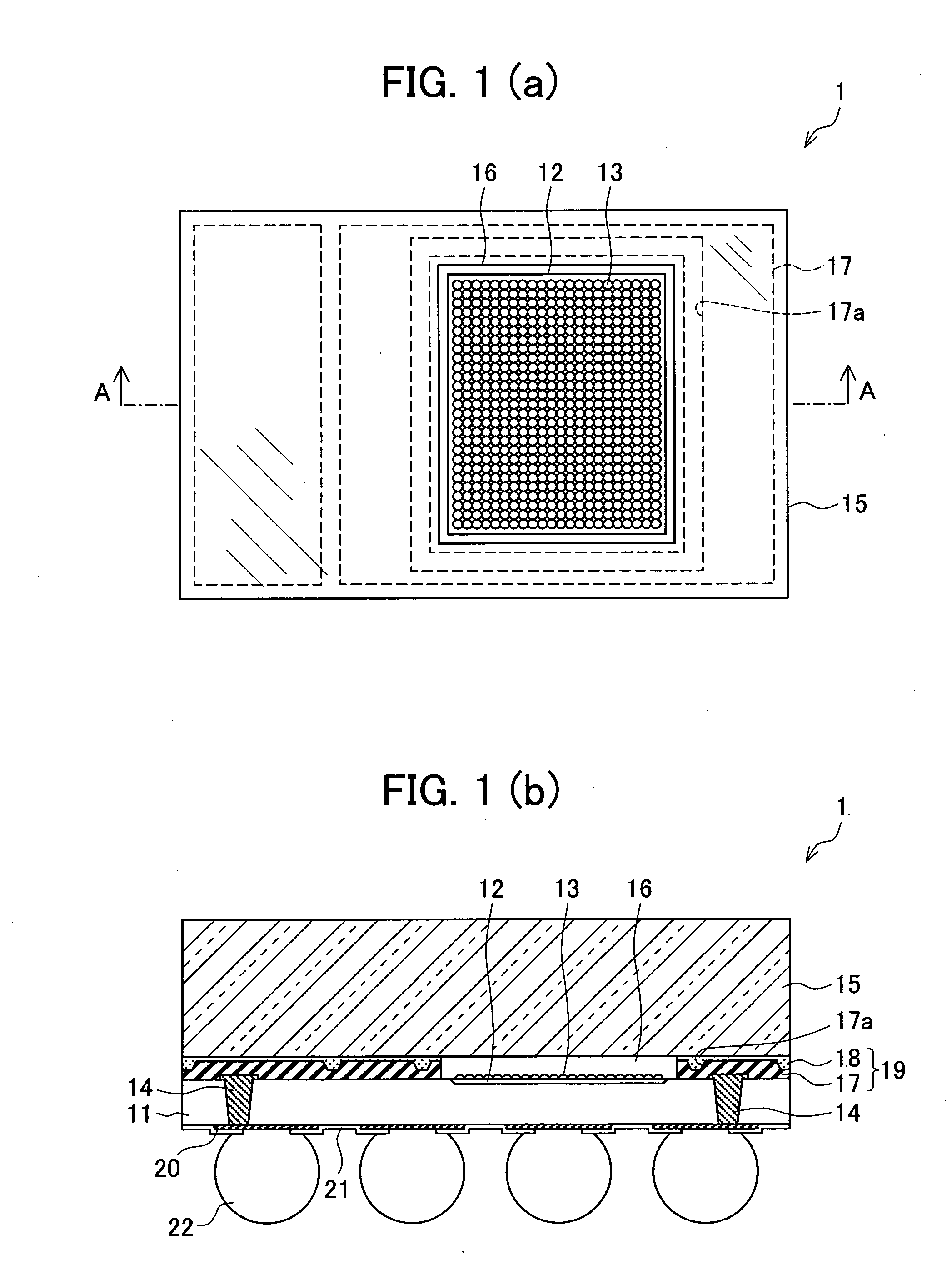
[0028] An embodiment of the present invention is explained below with reference to FIGS. 1 through 5.

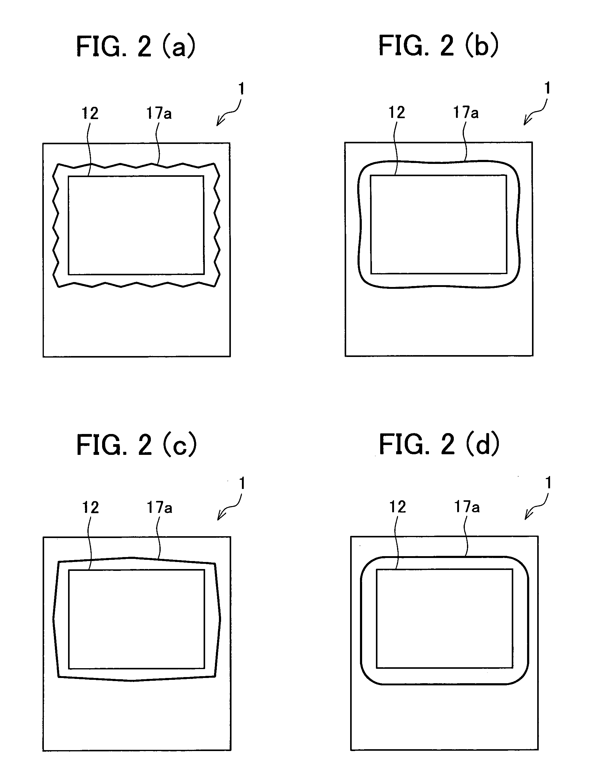
[0029]FIG. 1(a) is a plan view illustrating a structure of a semiconductor device 1 according to an embodiment of the present invention. FIG. 1(b) is a longitudinal sectional view illustrating the structure of the semiconductor device 1.

[0030] As illustrated in FIGS. 1(a) and 1(b), the semiconductor device 1 includes a semiconductor substrate 11 whose shape is rectangular when seen in a plan view. The semiconductor substrate 11 is a flat plate made of Si for example. An imaging element 12 whose shape is rectangular when seen in a plan view is formed on one side of the semiconductor substrate 11. The imaging element 12 is made by arraying a plurality of pixels that serve as a light reception sensor. A micro lens section 13 is formed on a face having the imaging element 12 thereon (corresponding to an active-element-formed face recited in claims). In order to increase a light collect...


PUM


Abstract

In a semiconductor device, a spacer layer is formed around an imaging element on a semiconductor substrate and a glass lid is combined to the spacer layer via an adhesive layer. A space is made between the semiconductor substrate and the glass lid so as to be positioned at a region where the imaging element is disposed. As a result, in forming a hollow section between a light transmitting material and an active element on the semiconductor substrate, it is unnecessary to apply a large load and to superimpose patterns when the light transmitting material is combined to the semiconductor substrate.

Description

[0001] This non-provisional application claims priority under 35 U.S.C. §119(a) on Patent Application No. 38395 / 2005 filed in Japan on Feb. 15, 2005, the entire contents of which are hereby incorporated by reference. FIELD OF THE INVENTION [0002] The present invention relates to a semiconductor device including (i) a semiconductor substrate in which a semiconductor element and a penetrating electrode are formed and (ii) a light transmitting material attached to the semiconductor substrate, the semiconductor device being preferably used for a light reception sensor such as a CCD and a CMOS imager, and to a production method thereof. BACKGROUND OF THE INVENTION [0003] A package of a light receiving sensor of a conventional CCD, a CMOS imager, or the like has a structure illustrated in FIG. 6. According to the structure, a semiconductor chip 101 is die-bonded, via a die bond material 117, in a hollow case 115 made of ceramic or resin, an electrode pad 109 is electrically connected with...

Claims


Application Information

Patent Timeline
Patent Type & Authority Applications(United States)
IPC IPC(8): H01L31/0232H01L27/14H04N5/335H04N5/369H04N5/372H04N5/374
CPCH01L27/14618H01L27/14625H01L27/14685H01L31/0203H01L2224/32225H01L2224/48091H01L2224/48227H01L2224/73265H01L2924/01078H01L2924/16195H01L2924/00014H01L2924/00H01L2924/00012H01L24/73F16B7/187E04H12/08F21S8/085
Inventor ONO, ATSUSHI
Owner SHARP KK
Why Eureka
Try Eureka