

Resin composition, heat-resistant resin paste and semiconductor device using these and method of preparing the same
a technology of resin paste and semiconductor device, which is applied in the direction of instruments, photomechanical devices, optics, etc., can solve the problems of warpage of substrates, warpage of frames, and small residual stress, and achieve the effect of warpage of the substrate, and reducing the size of the substra
- Summary
- Abstract
- Description
- Claims
- Application Information
AI Technical Summary
Benefits of technology
Problems solved by technology
Method used
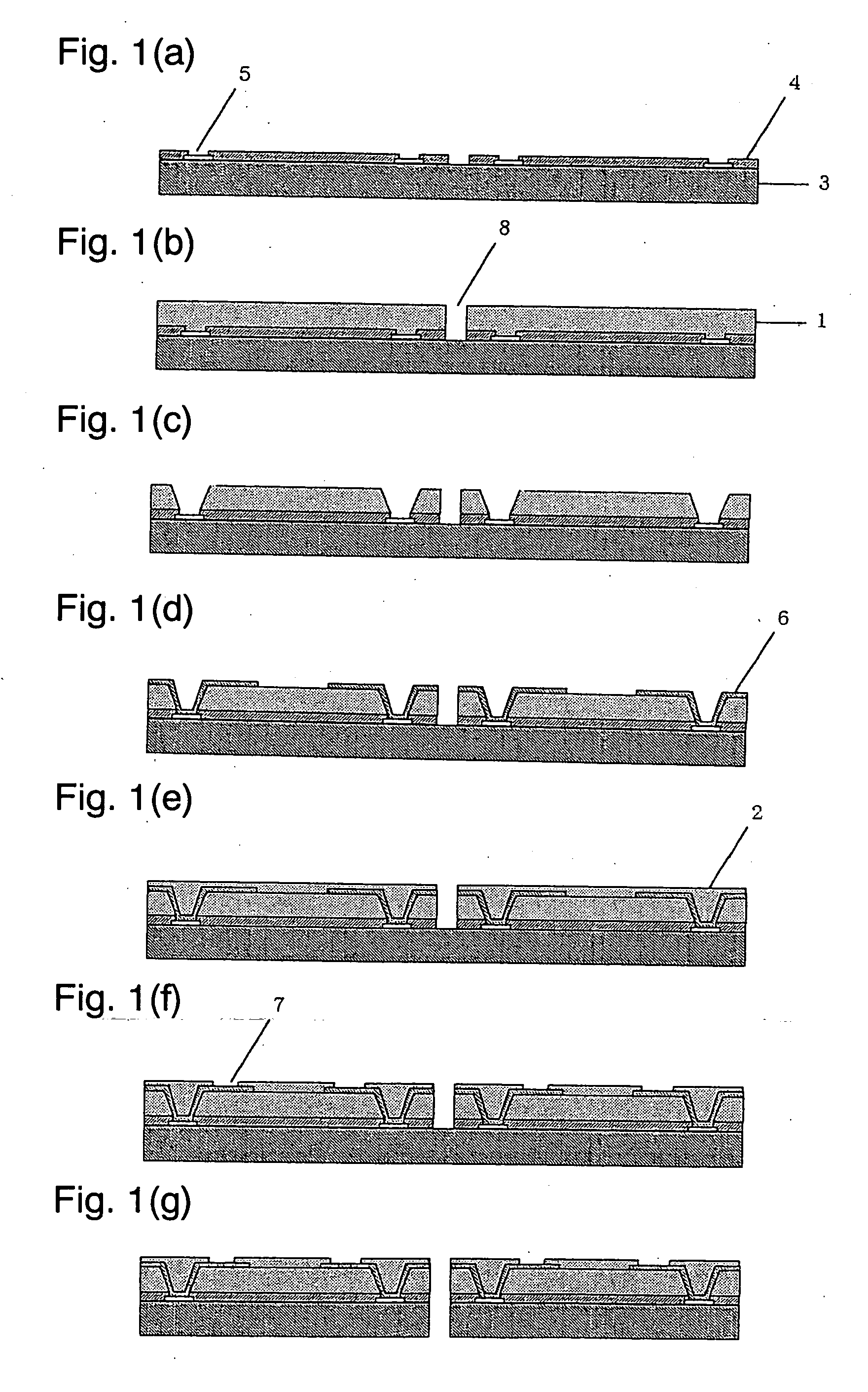
Image

Examples
example 1
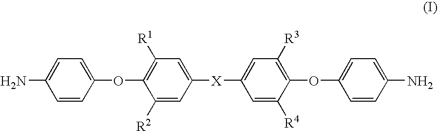
[0232] In a one-liter four-necked flask equipped with a thermometer, a stirrer, a nitrogen inlet tube, and a condenser equipped with an oil-water separator was charged 98.4 g (240 mmol) of 2,2-bis[4-(4-aminophenoxy)phenyl]propane (BAPP) under nitrogen atmosphere, and 700 g of N-methyl-2-pyrrolidone (NMP) was added thereto to dissolve the mixture. Next, while cooling the mixture not to exceed 20° C., 51.2 g (244 mmol) of trimellitic anhydride chloride (TAC) was added to the mixture. After stirring the mixture at room temperature for one hour, 30.3 g (300 mmol) of triethylamine was added while cooling the mixture not to exceed 20° C., and the resulting mixture was reacted at room temperature for 3 hours to produce a polyamic acid varnish. The resulting polyamic acid varnish was further subjected to dehydration reaction at 190° C. for 6 hours to produce a varnish of a polyether amide imide. This varnish of the polyether amide imide was poured into water and the resulting precipitates w...
example 2
[0238] Production of the resin composition and the semiconductor device, and the evaluations thereof were conducted in the same manner as in Example 1 except that, in a synthesis of a polyether amide imide which is soluble in a polar solvent at the room temperature, a diamine compound was changed to 93.3 g (216 mmol) of bis[4-(4-aminophenoxy)phenyl]phenyl]sulfone (BAPS) and 6.0 g (24 mmol) of 1,3-bis(aminopropyl)tetramethyldisiloxane. The results are shown in Table 1.
example 3
[0239] Production of the resin composition and the semiconductor device, and the evaluations thereof were conducted in the same manner as in Example 1 except that, in a synthesis of a polyether amide imide which is soluble in a polar solvent at the room temperature, a diamine compound was changed to 78.7 g (192 mmol) of 2,2-bis[4-(4-aminophenoxy)phenyl]propane (BAPP), 6.0 g (24 mmol) of 1,3-bis(aminopropyl)tetramethyldisiloxane and 4.8 g (24 mmol) of 4,4′-diaminodiphenyl ether, an acid compound was changed to 24.8 g (122 mmol) of isophthalic acid dichloride and 25.6 g (122 mmol) of trimellitic anhydride chloride. The results are shown in Table 1.
PUM
| Property | Measurement | Unit |
|---|---|---|
| viscosity | aaaaa | aaaaa |
| thixotropic coefficient | aaaaa | aaaaa |
| weight-loss temperature | aaaaa | aaaaa |
Abstract
Description
Claims
Application Information