Driving circuit of light emitting element

Inactive Publication Date: 2006-08-17
IND TECH RES INST
View PDF6 Cites 10 Cited by
  • Summary
  • Abstract
  • Description
  • Claims
  • Application Information

AI Technical Summary

Benefits of technology

[0011] It is the primary object of the invention to provide a driving circuit for a light emitting element, comprising a storage capacitor made of non-volatile material, which is capable of utilizing the hys

Problems solved by technology

Among all the design for optimizing the performance of displays, power-saving is alw

Method used


Image

  • Driving circuit of light emitting element
  • Driving circuit of light emitting element
  • Driving circuit of light emitting element

Examples


first embodiment

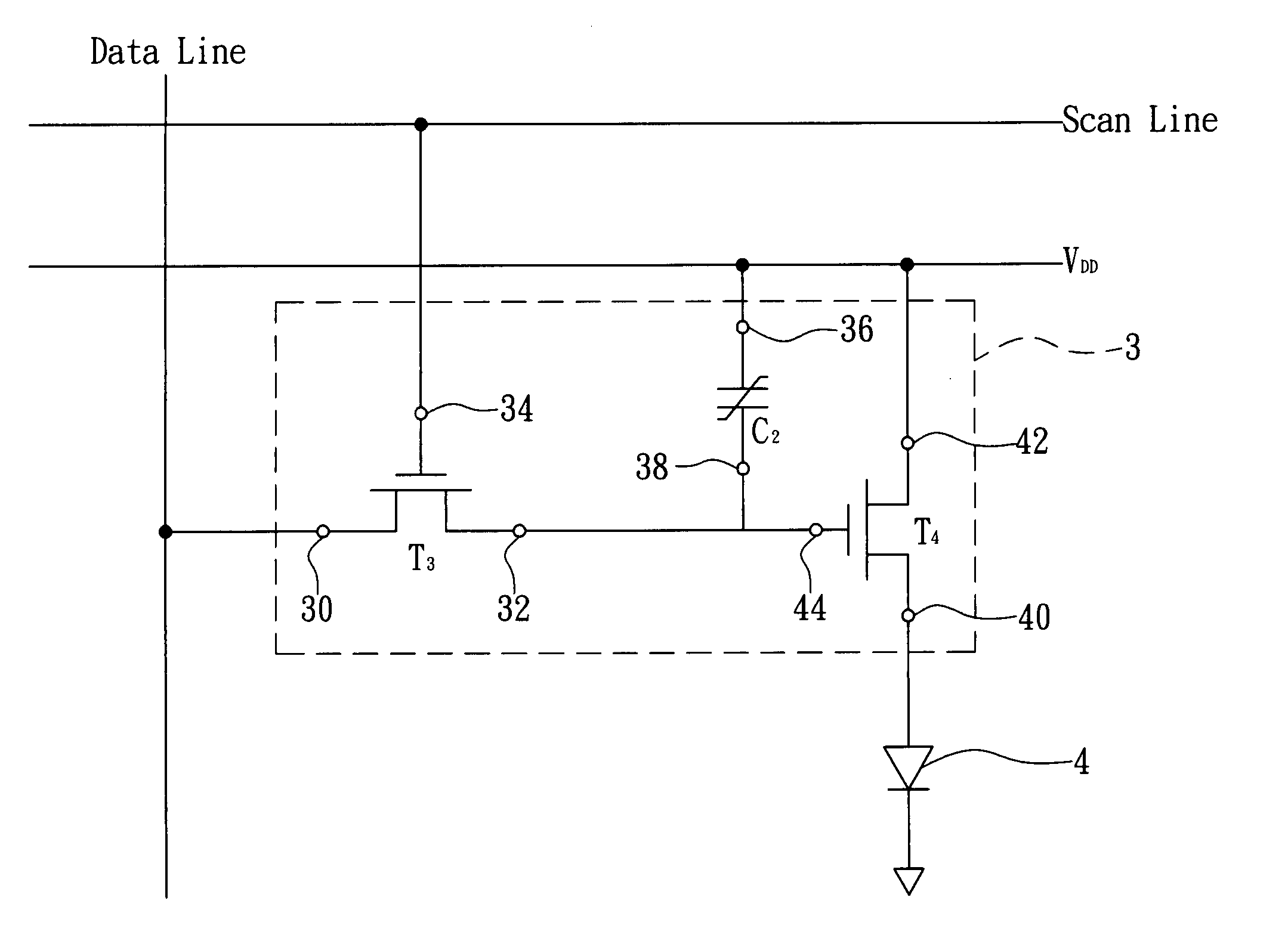
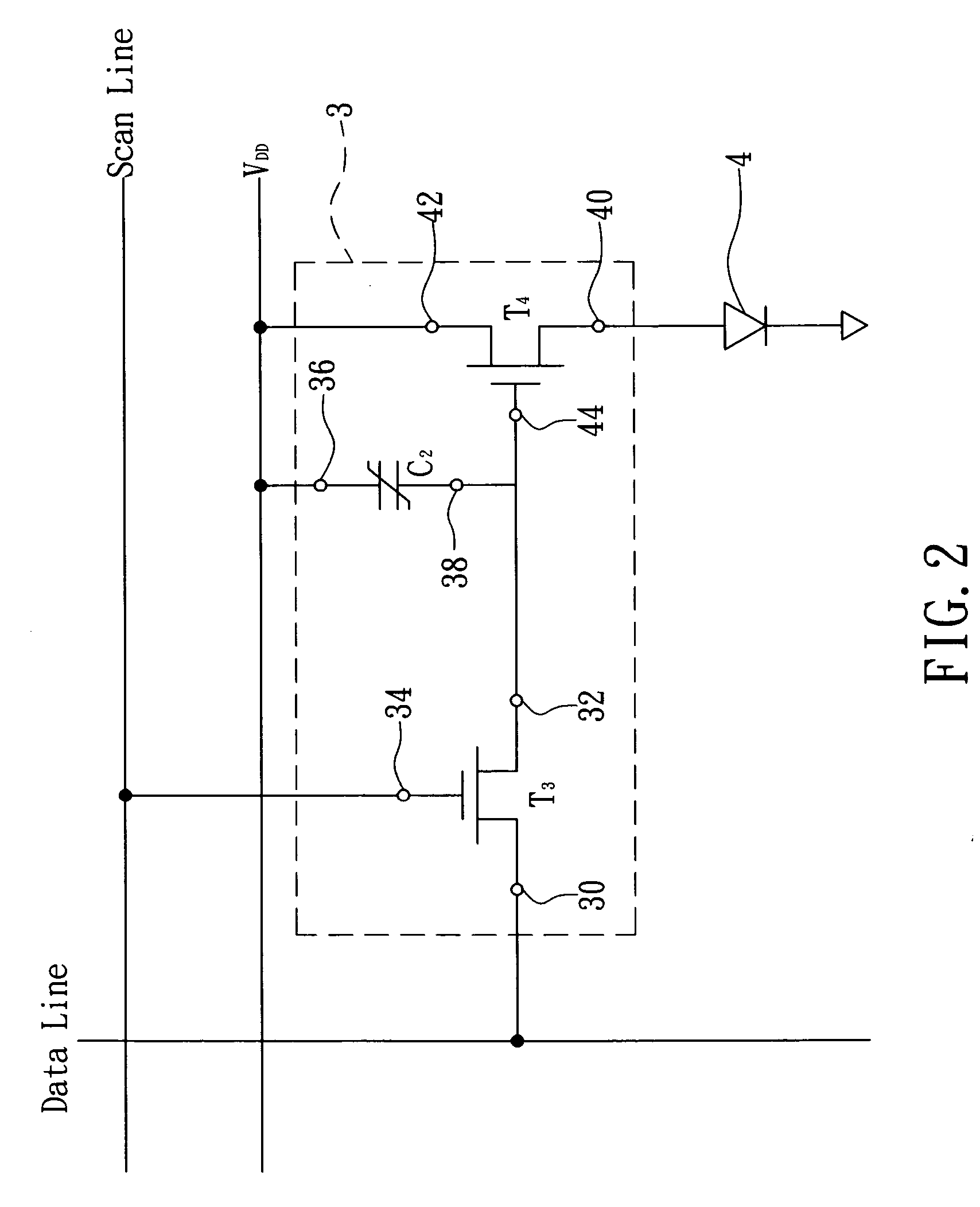
[0028] Please refer to FIG. 2, which is a schematic view of a driving circuit of light emitting element according to the invention. Similar to that shown in FIG. 1, the driving circuit 3 is electrically connected to a data line and a scan line, that is powered by a bias voltage VDD so as to drive a light emitting element 4, wherein the data line is further connected to a data driver and the scan line is further connected to a scan driver. The driving circuit 3 further comprises two transistor T3, T4, and a capacitor C2, wherein the gate 34 of the transistor T3 is electrically connected to the scan line while a node 30 of the drain / source of the transistor T3 is electrically connected to the data line, the gate 44 of the transistor T4 is electrically connected to another node 32 of the drain / source of the transistor T3 while a node 42 of the drain / source of the transistor T4 is electrically connected to the bias voltage VDD and another node 40 thereof is electrically connected to the...

second embodiment

[0030] Please refer to FIG. 3, which is a schematic view of a driving circuit of light emitting element according to the invention. The driving circuit 5 is electrically connected to a data line and a scan line, that is powered by a bias voltage VDD so as to drive a light emitting element 6, wherein the data line is further connected to a data driver and the scan line is further connected to a scan driver. The difference between the FIG. 3 and the FIG. 2 is that driving circuit 5 only comprises two transistors T5, T6, where transistor T6 is made of a non-volatile material such as a ferroelectric material.

[0031] As seen in FIG. 3, the gate 54 of the transistor T5 is electrically connected to the scan line while a node 50 of the drain / source of the transistor T5 is electrically connected to the data line, the gate 64 of the transistor T6 is electrically connected to another node 52 of the drain / source of the transistor T5 while a node 62 of the drain / source of the transistor T6 is ele...


PUM


Abstract

A driving circuit for a light emitting element, electrically connected to a data line and a scan line and powered by a bias voltage so as to drive the light emitting element, comprising: a first transistor, further comprising: a first gate, electrically connected to the scan line; and a first drain/source, having a first node electrically connected to the data line and a second node; and a second transistor, further comprising: a second gate, electrically connected to the second node of the first drain/source; and a second drain/source, having a first node electrically connected to the bias voltage, and a second node electrically connected to the light emitting element; wherein, an insulation layer and a layer of non-volatile material is formed successively between the semiconductor layer and the second gate of the second transistor.

Description

1. FIELD OF THE INVENTION [0001] The present invention relates to driving circuit of light emitting element, and more particularly, to a non-volatile driving circuit for driving light emitting elements. 2. BACKGROUND OF THE INVENTION [0002] As the rapid advance of technology propelling the development of electronic related industry, electronic products had become more and more intimate to our daily life, which is especially true to computers. No matter it is a desktop computer, or is a notebook computer, both require to use displays for showing information to users thereof. Hence, without notice, displays have become the electronic products that are used almost all the time in our modern life. [0003] As displays have becoming more and more closely related to our lives, the electronic related industry feels the need of optimizing the performance of displays so as to provide a more competitive and user friendly electronic product to the consumers. Among all the design for optimizing t...

Claims


Application Information

Patent Timeline
IPC IPC(8): G09G3/20
CPCG09G3/3233G09G2300/0842G09G2300/0847G09G2300/088G09G2330/022H01L27/3244H10K59/12
Inventor TSENG, HUAI-YUANYEH, YUNG-HUI
Owner IND TECH RES INST
Why Eureka
Try Eureka