Silicon nano wire having a silicon-nitride shell and method of manufacturing the same

a silicon nano wire and nano-nitride technology, applied in the direction of polycrystalline material growth, crystal growth process, transportation and packaging, etc., can solve the problems of low luminescence efficiency of less than 1%, limited use of photo luminescence method, and difficult to achieve, and achieve good light emission characteristics

Inactive Publication Date: 2006-08-17
SAMSUNG ELECTRONICS CO LTD
View PDF1 Cites 38 Cited by
  • Summary
  • Abstract
  • Description
  • Claims
  • Application Information

AI Technical Summary

Benefits of technology

[0012] The present invention may provide a silicon nano wire structure, as a low dimensional nano structure, the size of which can be readily controlled, and which has good light emitting characteristics, and a method of manufacturing the silicon nano wire structure.

Problems solved by technology

The former structure has a low luminescence efficiency of less than 1% due to the characteristics of crystalline silicon, and is limited to use for a photo luminescence method due to the difficulty of injecting current.
However, this remains difficult to achieve.

Method used


Image

  • Silicon nano wire having a silicon-nitride shell and method of manufacturing the same
  • Silicon nano wire having a silicon-nitride shell and method of manufacturing the same
  • Silicon nano wire having a silicon-nitride shell and method of manufacturing the same

Examples


Embodiment Construction

[0029] The present invention will now be described more fully with reference to the accompanying drawings in which exemplary embodiments of the invention are shown. Like reference numerals refer to like elements throughout the drawings.

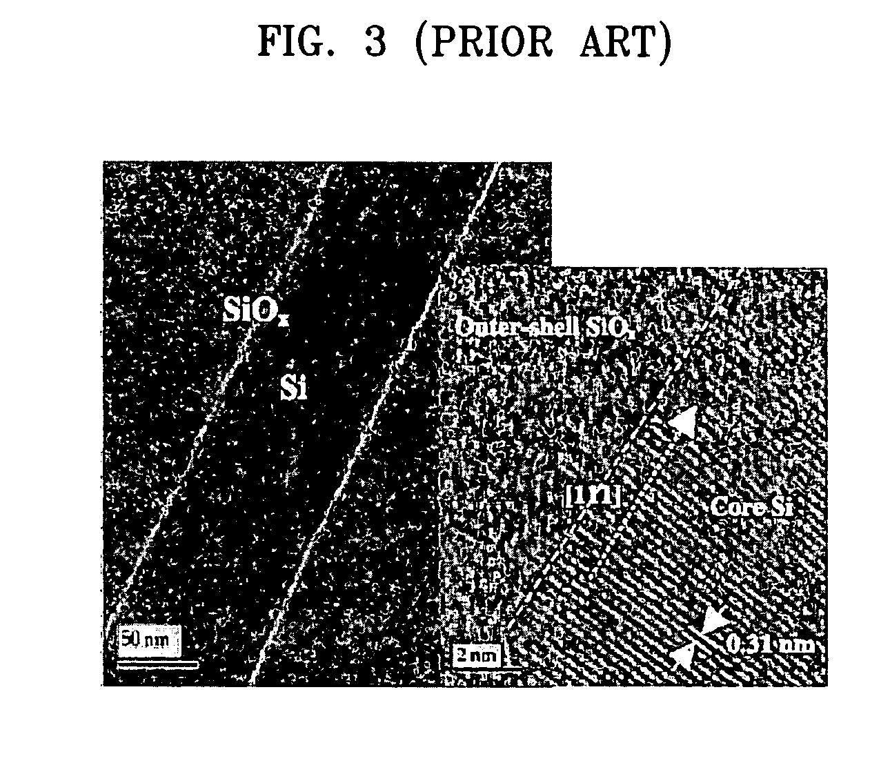
[0030]FIG. 3 is a SEM image of a conventional silicon nano wire having a silicon oxide shell. The silicon nano wire has a silicon core portion composed of crystalline silicon and a silicon oxide shell portion. The silicon oxide shell portion is generally formed by native oxidation and can also be formed by thermal oxidation. While the silicon oxide is formed at the surface of the silicon nano wire, as the silicon oxide shell portion grows, the diameter of the silicon core portion decreases, since the silicon oxide grows not only radially, but also grows toward the center of the silicon nano wire. However, the silicon oxide grows so rapidly that the diameter of the silicon nano wire using the silicon oxide shell portion cannot be controlled.

[0031] Al...


PUM

PropertyMeasurementUnit
temperatureaaaaaaaaaa
band gapaaaaaaaaaa
band gapaaaaaaaaaa

Abstract

Silicon nano wires having silicon nitride shells and a method of manufacturing the same are provided. Each silicon nano wire has a core portion formed of silicon, and a shell portion formed of silicon nitride surrounding the core portion. The method includes removing silicon oxide formed on the shell of the silicon nano wire and forming a silicon nitride shell.

Description

CROSS-REFERENCE TO RELATED PATENT APPLICATION [0001] This application claims the benefit of Korean Patent Application No. 10-2005-0012917, filed on Feb. 16, 2005, in the Korean Intellectual Property Office, the disclosure of which is incorporated herein in its entirety by reference. BACKGROUND OF THE DISCLOSURE [0002] 1. Field of the Disclosure [0003] The present disclosure relates to a silicon nano wire, and more particularly, to a silicon nano wire having a silicon-nitride shell and a method of manufacturing the same. [0004] 2. Description of the Related Art [0005] Since the structure of carbon nano tubes was reported (S. Iijima. Nature (London) 1991, 354, 65) in 1991, further studies have investigated methods of synthesizing and using nano structures having dimensions of less than 100 nm. Nano structures are made from inorganic materials, such as single component semiconductors (Si, Ge, and B), III-V group compound semiconductors (GaN, GaAs, GaP, InP, and InAs), II-Vi group compo...

Claims


Application Information

Patent Timeline
Patent Type & Authority Applications(United States)
IPC IPC(8): D02G3/00
CPCB82Y30/00C30B11/12Y10T428/2933C30B29/06C30B29/60C30B25/00B82B1/00B82B3/00B82Y20/00
Inventor LEE, EUN-KYUNGCHOI, BYOUNG-IYONG
Owner SAMSUNG ELECTRONICS CO LTD
Why Eureka
Try Eureka