Method of fabricating polycrystalline silicon thin film for improving crystallization characteristics and method of fabricating liquid crystal display device using the same

Active Publication Date: 2006-08-24
LG DISPLAY CO LTD
View PDF17 Cites 7 Cited by
  • Summary
  • Abstract
  • Description
  • Claims
  • Application Information

AI Technical Summary

Benefits of technology

[0022] Another object of the present invention is to provide a method of fabricating a polycrystalline thin film transistor having increased electrical characteristics.

Problems solved by technology

However, the field effect mobility of the amorphous silicon thin film transistor of about 1 cm2 / Vsec prevents its use in peripheral circuits that apply signals to the pixel region, since peripheral circuits operate at more than 1 MHz.
However, there are many defects in the grains.
Although not as bad as grain boundaries in a polycrystalline thin film transistor, these defects are a bad influence on a performance of a polycrystalline silicon thin film transistor.
However, a distribution density of the crystal nucleus N is not uniform.
Further, the size of the grains are not uniform.
Thus, there will be a non-uniformity of picture quality across an entire display panel.
Also, if a channel of a thin film transistor is not formed in parallel with a longitudinal direction of grains (that is, a direction in which the number of times to meet with a grain boundary is less), a high mobility can not be obtained even if a grain size is large.
This direction-dependent characteristic of grains causes problems, especially in a thin film transistor of a driving circuit region.

Method used


Image

  • Method of fabricating polycrystalline silicon thin film for improving crystallization characteristics and method of fabricating liquid crystal display device using the same
  • Method of fabricating polycrystalline silicon thin film for improving crystallization characteristics and method of fabricating liquid crystal display device using the same
  • Method of fabricating polycrystalline silicon thin film for improving crystallization characteristics and method of fabricating liquid crystal display device using the same

Examples


first embodiment

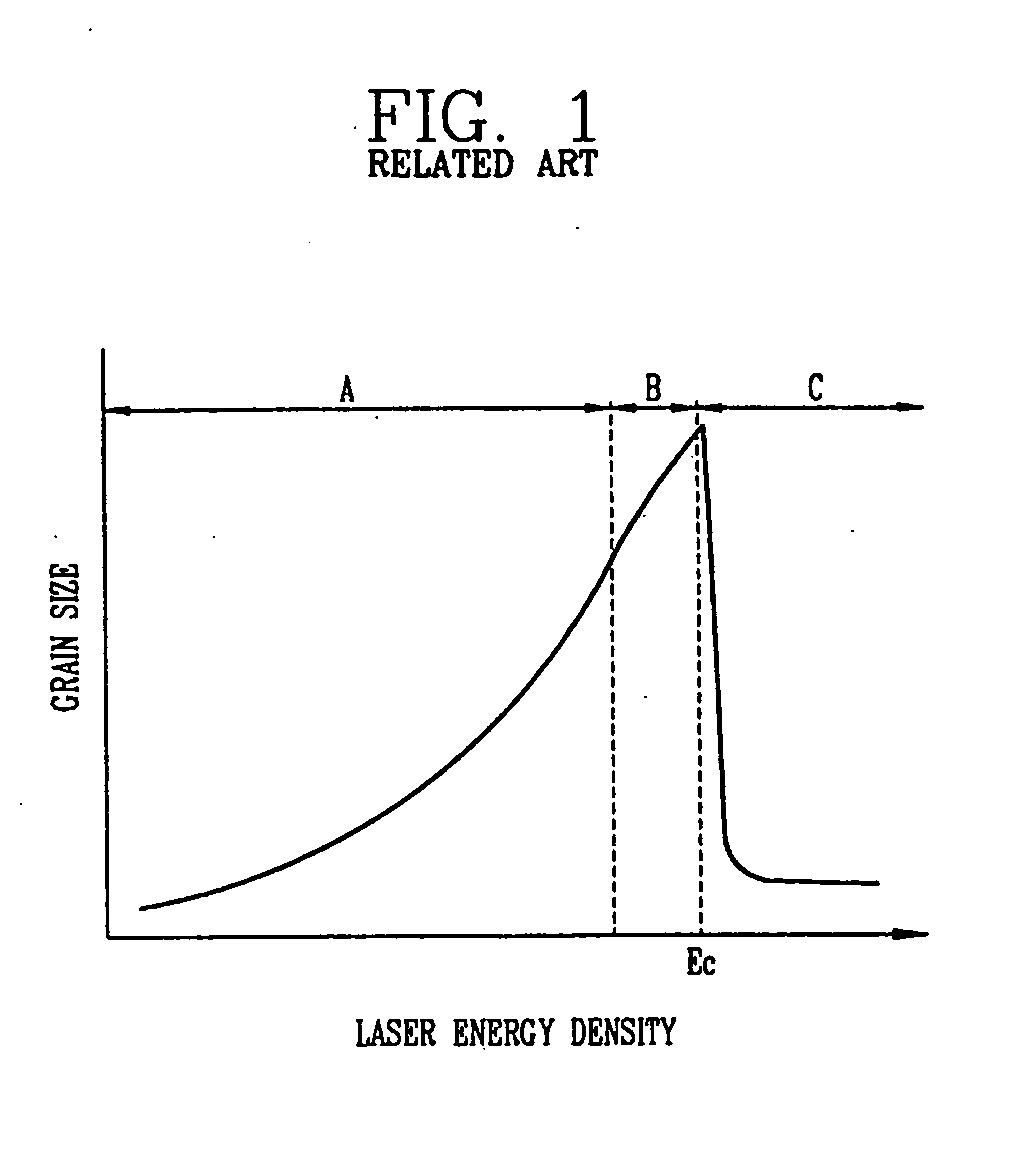
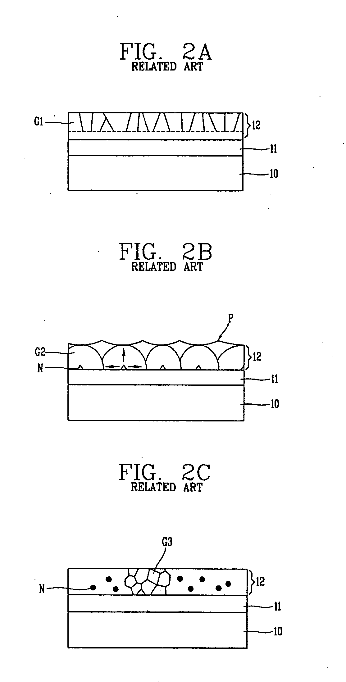
[0042]FIGS. 3A to 3D are flow charts showing a crystallization method according to the present invention, which shows a lateral crystallization method. In said embodiment, a sequential lateral solidification (SLS) technique was used as the lateral crystallization method. However, another lateral crystallization methods, such as a selectively enlarging laser crystallization (SELAX) or a metal induced lateral crystallization (MILC), can be used. The sequential lateral solidification is a technique based upon the fact that a silicon grains grow in a vertical direction at an interface between a liquid silicon and a solid silicon as described in Robert S. Sposilli, M. A. Crowder, and James S. Im, Material Research Society Symposium Process Vol. 452, 956˜957, 1997. According to the sequential lateral solidification technique, silicon grains are laterally grown with a certain length by properly controlling a laser energy density and a laser irradiation scope to thereby crystallize amorphou...

second embodiment

[0053]FIGS. 5A to 5D are flow charts showing a fabrication method of a polycrystalline silicon thin film according to the present invention. In said preferred-embodiment, a crystallization process is performed by using an amorphous silicon thin film having a thickness of 1000˜2000 Å, which is thicker than a general thickness as an active layer of a thin film transistor. If a thickness of the amorphous silicon thin film is thick, frequency of sub grain boundaries are decreased and a polycrystalline silicon thin film having a large grain size can be obtained.

[0054] As shown in FIG. 5A, an amorphous silicon thin film 212 to be used in crystallization is deposited to a certain thickness on a buffer layer 211, which is on a substrate 210. Generally, any one of a variety of methods can deposit the amorphous silicon thin film 212. Such methods include low pressure chemical vapor deposition (LPCVD) and plasma enhanced vapor deposition (PECVD).

[0055] In the case that the amorphous silicon t...


PUM


Abstract

A crystallization method of an amorphous semiconductor layer includes providing an amorphous semiconductor layer having a first thickness, crystallizing the amorphous semiconductor layer in a first direction, partially reducing the crystallized semiconductor layer to a second thickness less than the first thickness and crystallizing the etched semiconductor layer in a second direction.

Description

[0001] The present invention claims the benefit of Korean Patent Application No. 200344002 filed in Korea on Jun. 30, 2003, which is hereby incorporated by reference. BACKGROUND OF THE INVENTION [0002] 1. Field of the Invention [0003] The present invention relates to a method of fabricating a polycrystalline silicon thin film, and more particularly, to a method of fabricating a polycrystalline silicon thin film for improving crystallization characteristics and a method of fabricating a liquid crystal display device using the same. [0004] 2. Description of the Related Art [0005] Recently, because of the need for an information display and a high demand for using a portable information systems, light and thin film type flat panel display (FPD) devices have been actively being researched and commercialized such that the conventional device of a cathode ray tube (CRT) is being replaced. Among these flat panel display devices, a liquid crystal display (LCD) device is used for displaying ...

Claims


Application Information

Patent Timeline
IPC IPC(8): H01L21/84G02F1/136H01L21/20H01L21/336H01L21/77H01L27/12H01L29/04H01L29/786
CPCH01L21/02532H01L21/0268H01L21/02691H01L27/1285H01L27/1296H01L29/04H01L29/66757H01L29/78675G02F1/136
Inventor KIM, SANG HYUN
Owner LG DISPLAY CO LTD
Why Eureka
Try Eureka