Polishing apparatus and related polishing methods

a technology of polishing apparatus and polishing method, which is applied in the direction of grinding machine components, manufacturing tools, lapping machines, etc., can solve the problems of unevenness (i.e., step differences) and non-uniform polishing, and achieve the effect of uniform polishing thickness of an obj

Inactive Publication Date: 2006-08-24
SAMSUNG ELECTRONICS CO LTD
View PDF12 Cites 200 Cited by
  • Summary
  • Abstract
  • Description
  • Claims
  • Application Information

AI Technical Summary

Benefits of technology

[0014] Embodiments of the present invention provide polishing apparatus and / or polishing methods capable of maintaining substantially uniform polishing thickness of an object to be polished by generating pressure that can be substantially uniformly applied to an object (such as a wafer) to be polished.

Problems solved by technology

Also, upon simultaneous formation of the metal buried wirings whose widths may be different from each other, if metal film is deposited on a plurality of grooves whose widths are different, then unevenness (i.e., step differences) may be undesirably formed on the surface of the metal film.
Unfortunately, the polishing apparatus having the foregoing construction may have problems that contribute to non-uniform polishing.

Method used


Image

  • Polishing apparatus and related polishing methods
  • Polishing apparatus and related polishing methods
  • Polishing apparatus and related polishing methods

Examples


Embodiment Construction

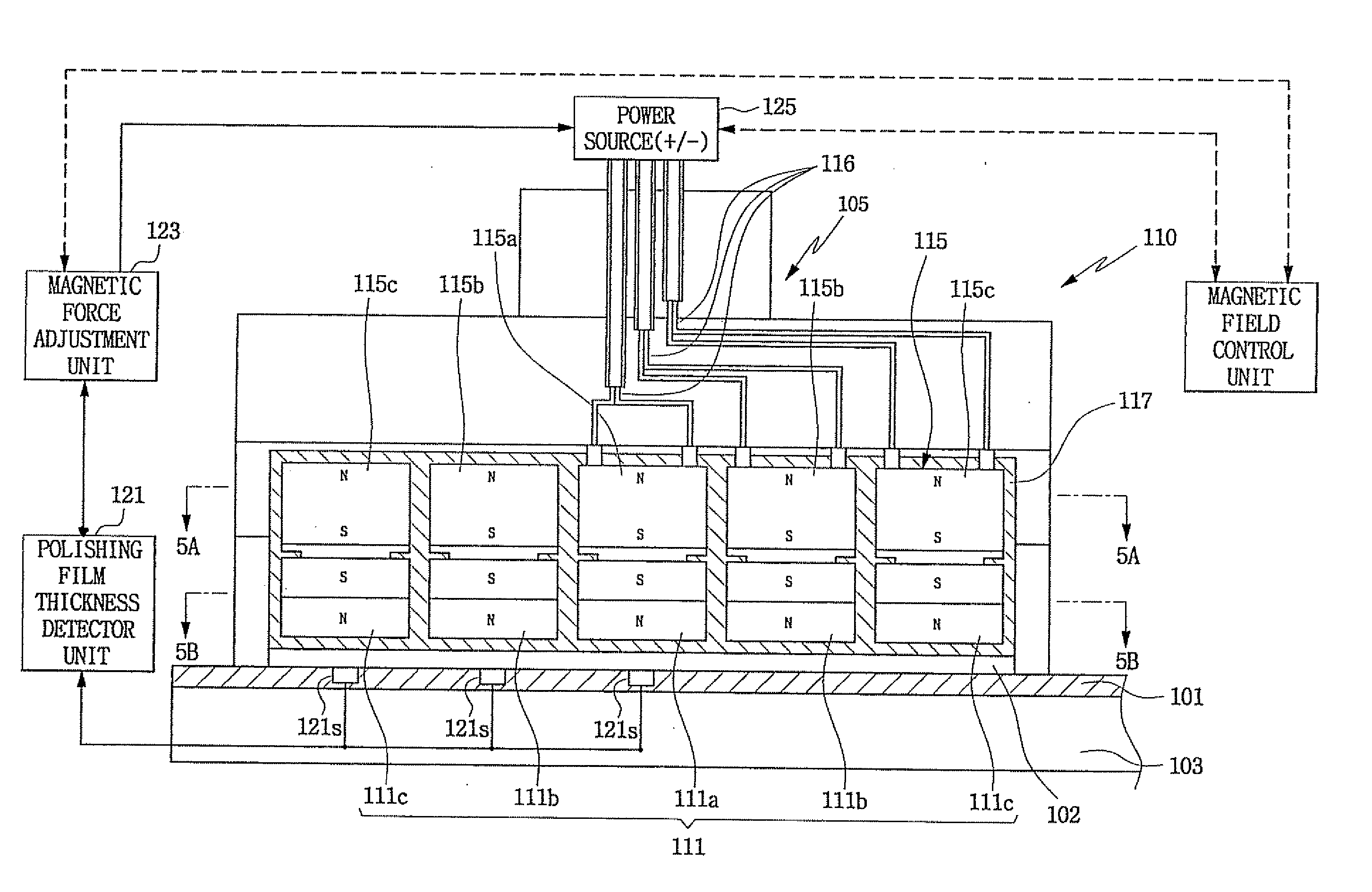
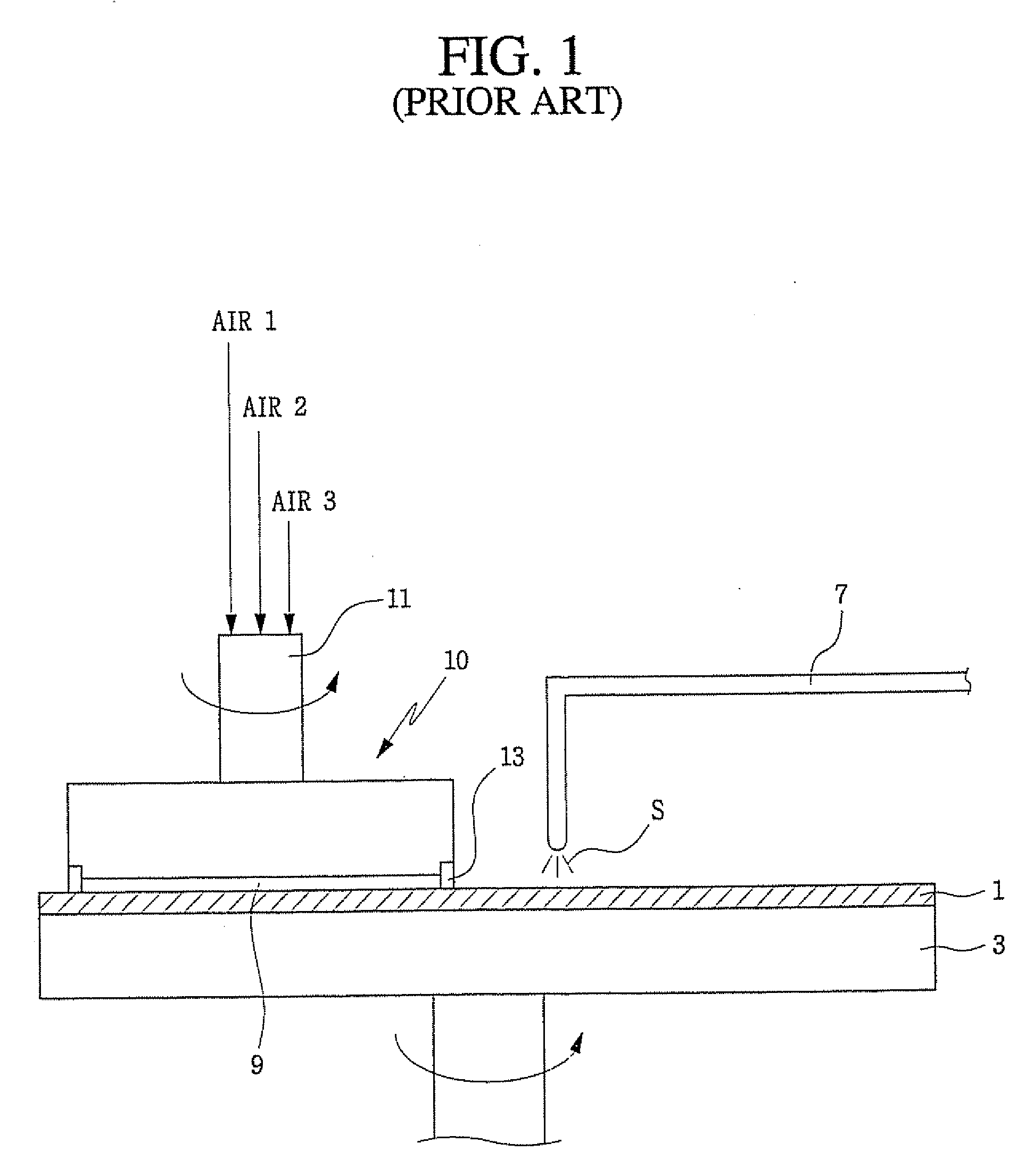
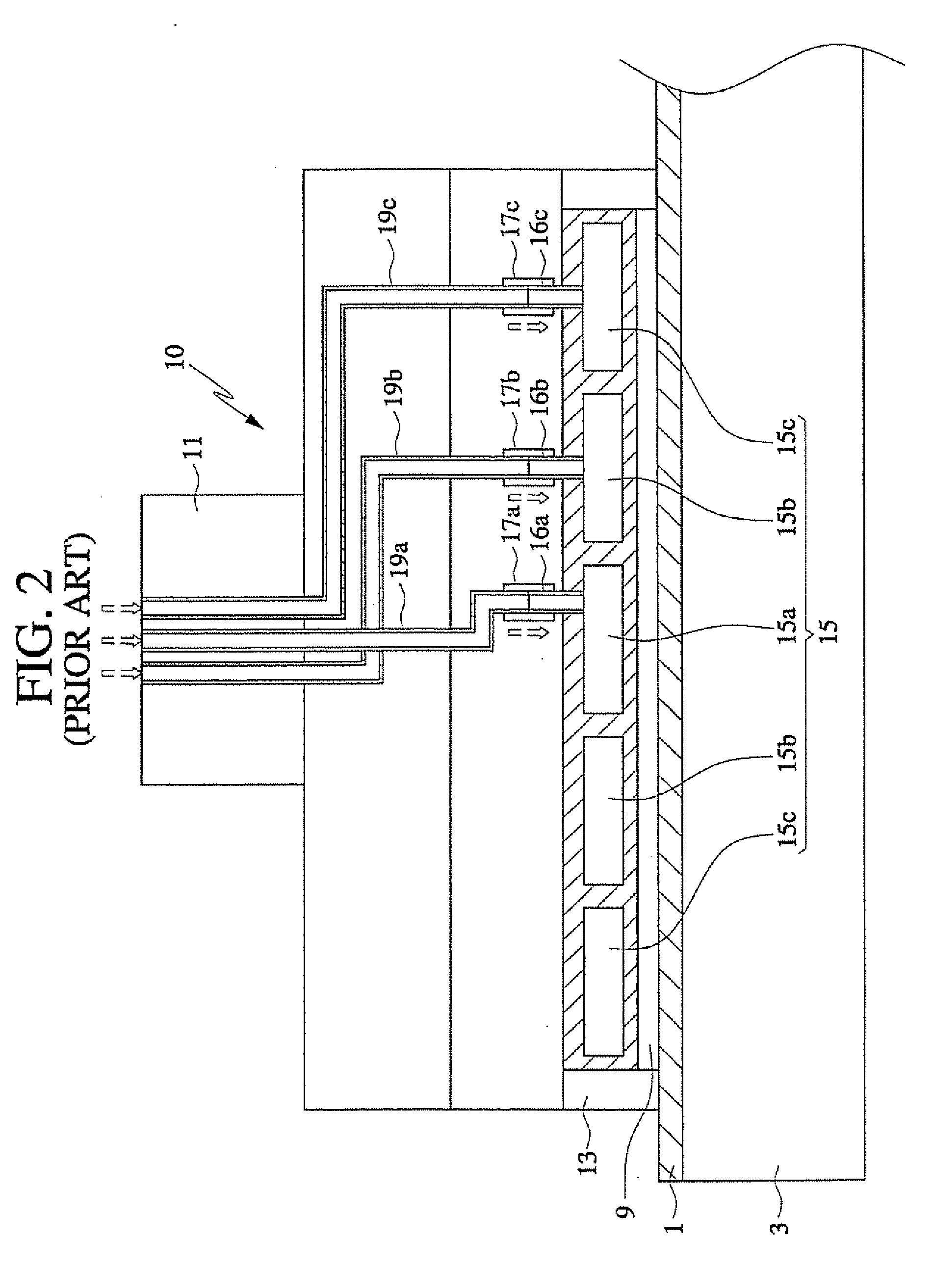
[0036] The present invention will now be described more fully hereinafter with reference to the accompanying drawings, in which embodiments of the invention are shown. Like numbers refer to like elements. In the figures, certain features, layers or components may be exaggerated for clarity. Also, in the figures, broken lines indicate optional features or components unless stated otherwise. When a layer is referred to as being “on” another layer or substrate, it can be directly on the other layer or substrate, or intervening layers, films, coatings and the like may also be present unless the word “directly” is used which indicates that the feature or layer directly contacts the feature or layer. In addition, spatially relative terms, such as “beneath”, “below”, “lower”, “above”, “upper” and the like, may be used herein for ease of description to describe one element or feature's relationship to another element(s) or feature(s) as illustrated in the figures. It will be understood that...


PUM

PropertyMeasurementUnit
magnetic fieldaaaaaaaaaa
magnetic forceaaaaaaaaaa
pressureaaaaaaaaaa

Abstract

Polishing apparatus and related methods employ aligned first and second magnetic field sources to adjust the compressive force and / or pressure applied by a carrier head against a target workpiece (such as a wafer) by selectively and controllably generating a repellant or attractive force between the two magnetic field sources.

Description

RELATED APPLICATION [0001] This application is a divisional of U.S. patent Ser. No. 10 / 715,314, filed Nov. 17, 2003, which claims the benefit of priority of Korean Patent Application Serial No. 2003-1690, filed on Jan. 10, 2003, the contents of which are hereby incorporated by reference herein in their entirety.FIELD OF THE INVENTION [0002] The present invention relates to polishing apparatus and methods of polishing, and more particularly to polishing apparatus and methods capable of reducing non-uniformity of thickness of an object to be polished. The apparatus and methods may be particularly suitable for use with wafers and / or structures comprising semiconductor substrates. BACKGROUND OF THE INVENTION [0003] Typically, when buried metal wiring such as Cu, Damascene, etc., is formed through planarized metal film (such as Cu, W, Al) deposited on a target substrate, such as a semiconductor substrate, CMP (Chemical Mechanical Polishing) can be used. [0004] Also, upon simultaneous for...

Claims


Application Information

Patent Timeline
Patent Type & Authority Applications(United States)
IPC IPC(8): B24B51/00B24B49/00B24B1/00B24B37/005B24B37/30B24B49/16H01L21/304
CPCB24B1/005B24B37/30B24B49/16H01L21/304
Inventor PARK, MOO-YONGHAH, SANG-ROKKIM, JONG-GYOONSON, HONG-SEONGHAN, JA-HYUNG
Owner SAMSUNG ELECTRONICS CO LTD
Why Eureka
Try Eureka