Semiconductor device allowing modulation of a gain coefficient and a logic circuit provided with the same

a technology of gain coefficient and semiconductor element, which is applied in the field of field-effect transistors, can solve the problems of unstable production quality, increased fabrication cost and production cost, and reduced yield, so as to reduce the variation in characteristics of the fabricated semiconductor element, reduce the cost of manufacturing, and increase the production cos

Inactive Publication Date: 2006-08-31
KENZAN
View PDF9 Cites 0 Cited by
  • Summary
  • Abstract
  • Description
  • Claims
  • Application Information

AI Technical Summary

Benefits of technology

[0010] Preferably, occurrence of the strong electric field region and the weak electric field region partially changes a direction of the electric field in the whole channel region formed by the first and second gates, and this change in electric field direction modulates the effective gate length and gate width in the whole channel region.
[0027] The semiconductor element according to the invention can modulate a gain coefficient β in an analog manner with high accuracy in accordance with a voltage applied to the second gate (control gate), which is provided in addition to the ordinary first gate. Further, the semiconductor element can be produced easily by conventional process techniques, and thereby can be incorporated into various kinds of conventional LSIs formed of MOS circuits. Therefore, it is possible to achieve on-chip mechanisms, which can correct variations in characteristics by automatically modulating or adjusting element parameters, in various kinds of semiconductor integrated circuits.
[0028] In particular, not only the first gate but also the second gate (control gate) has the geometry defined only by a group of straight lines each extending in one of perpendicular directions. Therefore, it is possible to reduce variations in characteristics during fabrication which may be caused by processing for oblique lines during subminiature processing of the semiconductor devices, so that a fabrication efficiency can be improved. In other words, a portion defined by an oblique line is eliminated from the from of the control gate so that fabricating quality of the semiconductor elements can be stable, and increase in fabrication cost can be prevented.

Problems solved by technology

Therefore, variations in characteristics due to variations in size of elements result in disadvantageous lowering of yields.
This results in difficulty in gate preparation, and thus results in increases in fabrication cost and unstable production quality.
More specifically, the above difficulty causes variations in characteristics of the fabricated semiconductor elements.

Method used


Image

  • Semiconductor device allowing modulation of a gain coefficient and a logic circuit provided with the same
  • Semiconductor device allowing modulation of a gain coefficient and a logic circuit provided with the same
  • Semiconductor device allowing modulation of a gain coefficient and a logic circuit provided with the same

Examples


first embodiment

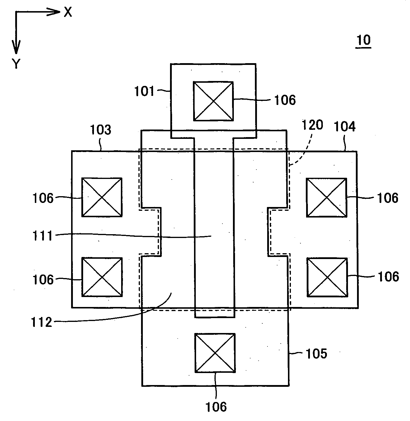
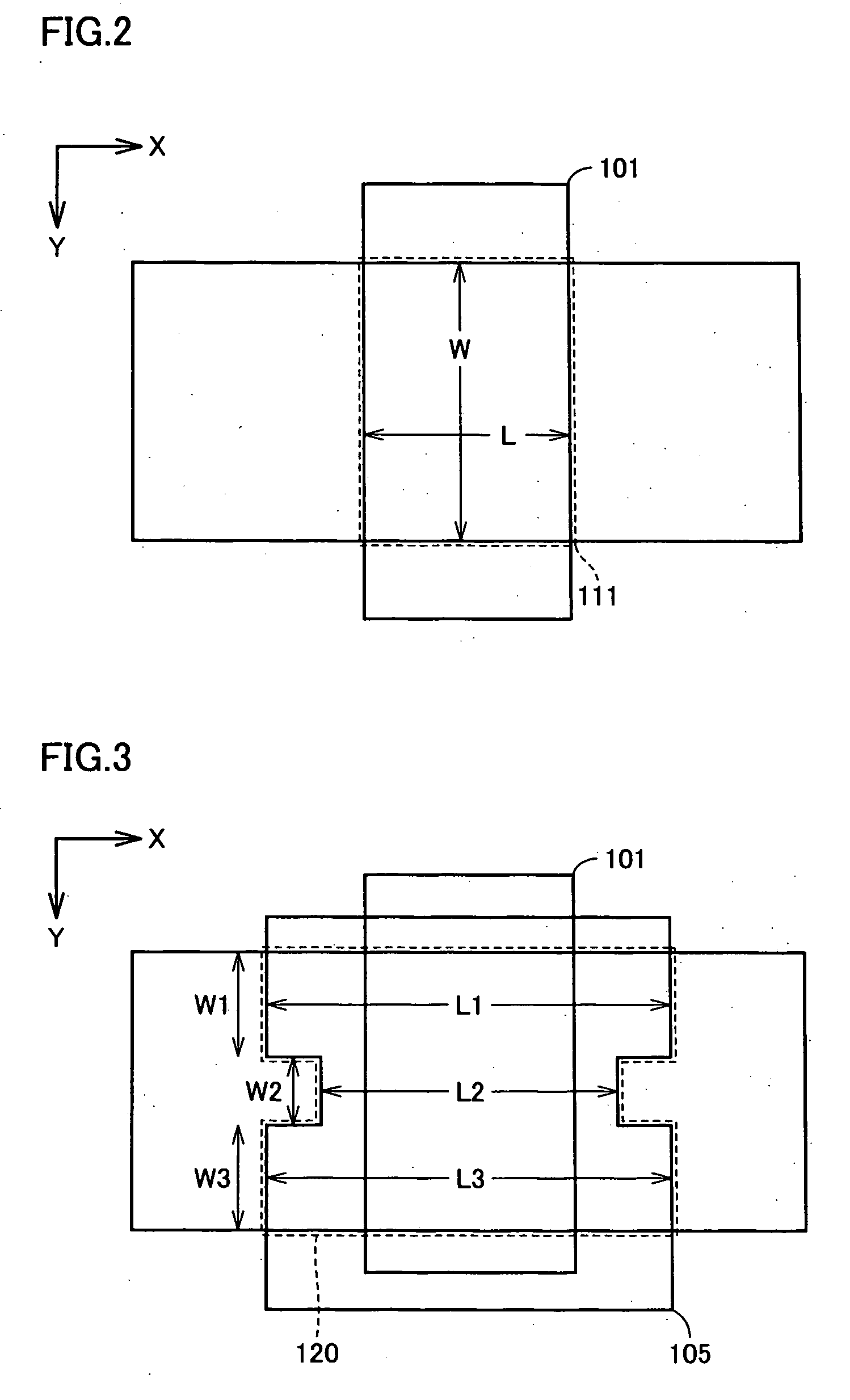
[0046] FIGS. 1 to 3 show a planar layout of a semiconductor element according to a first embodiment of the invention.

[0047] Referring to FIG. 1, a semiconductor element 10 according to a first embodiment includes an ordinary MOS gate 101, which will be merely referred to as a “MOS gate” hereinafter, a drain 103, a source 104 and a control gate 105, which is additionally employed according to the invention. MOS gate 101, drain 103, source 104 and control gate 105 are provided with contacts 106 for leading electrodes. Between drain 103 and source 104, MOS gate 101 forms a channel region 111, and control gate 105 forms a channel region 112. MOS gate 101 and control gate 105 are arranged such that channel regions 111 and 112 may have geometrical continuity.

[0048] In the following description, a direction along a gate length and a direction along a gate width of rectangular MOS gate 101 will be referred to as an X-direction and a Y-direction, respectively. Thus, MOS gate 101 has planar...

second embodiment

[0080]FIG. 9 shows a planar layout of a semiconductor element according to a second embodiment.

[0081] Referring to FIG. 9, a semiconductor element 11 according to the second embodiment has MOS gate 101, drain 103, source 104, control gate 105 and contacts 106, similarly to semiconductor element 10 of the first embodiment. Semiconductor element 11 according to the second embodiment differs from semiconductor element 10 only in the geometry of control gate 105. Therefore, the fabrication process and fabricating conditions of semiconductor element 11 can be similar to those of semiconductor element 10 according to the first embodiment.

[0082] Control gate 105 has such planar geometry that interrupting central portion of a region overlapping with ordinary gate 101 in a plan view, and is present in other portions. Thus, the gate length of control gate 105 is different between the central portion (interrupting portion) and the other portions. In semiconductor element 12, control gate 105...

third embodiment

[0086]FIG. 10 shows a planar layout of a semiconductor element according to a third embodiment of the invention.

[0087] Referring to FIG. 10, a semiconductor element 12 according to the third embodiment has MOS gate 101, drain 103, source 104, control gate 105 and contacts 106, similarly to semiconductor element 10 of the first embodiment. Semiconductor element 12 according to the third embodiment differs from semiconductor element 10 only in the geometry of control gate 105. Therefore, the fabrication process and fabricating conditions of semiconductor element 12 can be similar to those of semiconductor element 10 of the first embodiment.

[0088] In semiconductor element 12 of the third embodiment, control gate 105 has T-shaped geometry in a plan view. T-shaped control gate 105 is located in a region between drain 103 and source 104, and covers rectangular MOS gate 101 in a plan view. In semiconductor element 12, control gate 105 has planar geometry defined only by a group of straig...


PUM


Abstract

In addition to ordinary MOS gate, drain and source, a semiconductor element includes a control gate having geometry, which is defined only by a group of straight lines along a rectangular form of the MOS gate, is not defined by an oblique line and provides a nonuniform gate length at least in one of regions aligned in a direction of a gate width. A channel region formed by the control gate provides a region of strong electric fields and a region of weak electric fields. Consequently, a conductance of a whole channel region formed by the MOS gate and the control gate, i.e., a gain coefficient β of the semiconductor element can be modulated in accordance with voltages applied to the MOS gate and the control gate.

Description

BACKGROUND OF THE INVENTION [0001] 1. Field of the Invention [0002] The present invention relates to a semiconductor element, and particularly to a field-effect transistor, of which gain coefficient β can be modulated in an analog manner as well as a logic circuit provided with the same. [0003] 2. Description of the Background Art [0004] Semiconductor devices except for some special semiconductor elements have employed tri-electrode structures over about thirty years since these were invented. In a conventional semiconductor element, characteristics (gain coefficient β) depend on geometrical sizes set in a design stage, and therefore cannot be changed in a later stage. Thus, the gain coefficient β, which is a kind of unique characteristics of the semiconductor element, is fixed. Therefore, variations in characteristics due to variations in size of elements result in disadvantageous lowering of yields. [0005] For overcoming the above, International Application Publication No. WO02 / 05...

Claims


Application Information

Patent Timeline
Patent Type & Authority Applications(United States)
IPC IPC(8): H01L29/76H01L27/092H01L21/336H01L21/8234H01L21/8238H01L27/088H01L29/423H01L29/78
CPCH01L29/4238H01L29/66484H01L29/7832
Inventor HIROTSU, FUSAYOSHIHIROTSU, JUNICHI
Owner KENZAN
Why Eureka
Try Eureka