

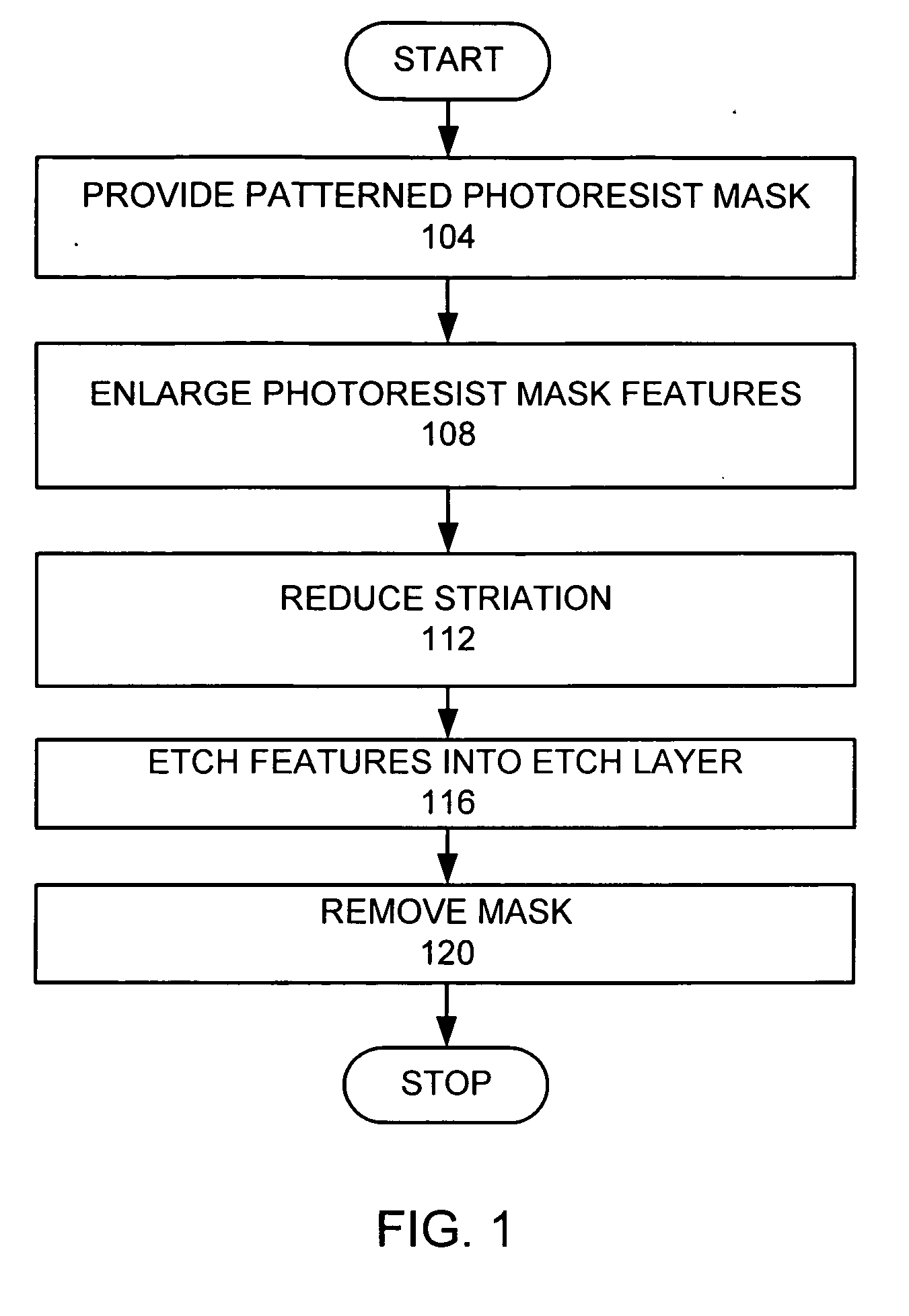
Etch with striation control
a technology of etching and control, applied in the direction of semiconductor devices, basic electric elements, electrical apparatus, etc., can solve the problems of cd limitation and striation, and achieve the effect of reducing the striation of photoresist features
- Summary
- Abstract
- Description
- Claims
- Application Information
AI Technical Summary
Benefits of technology
Problems solved by technology
Method used
Image

Examples
example
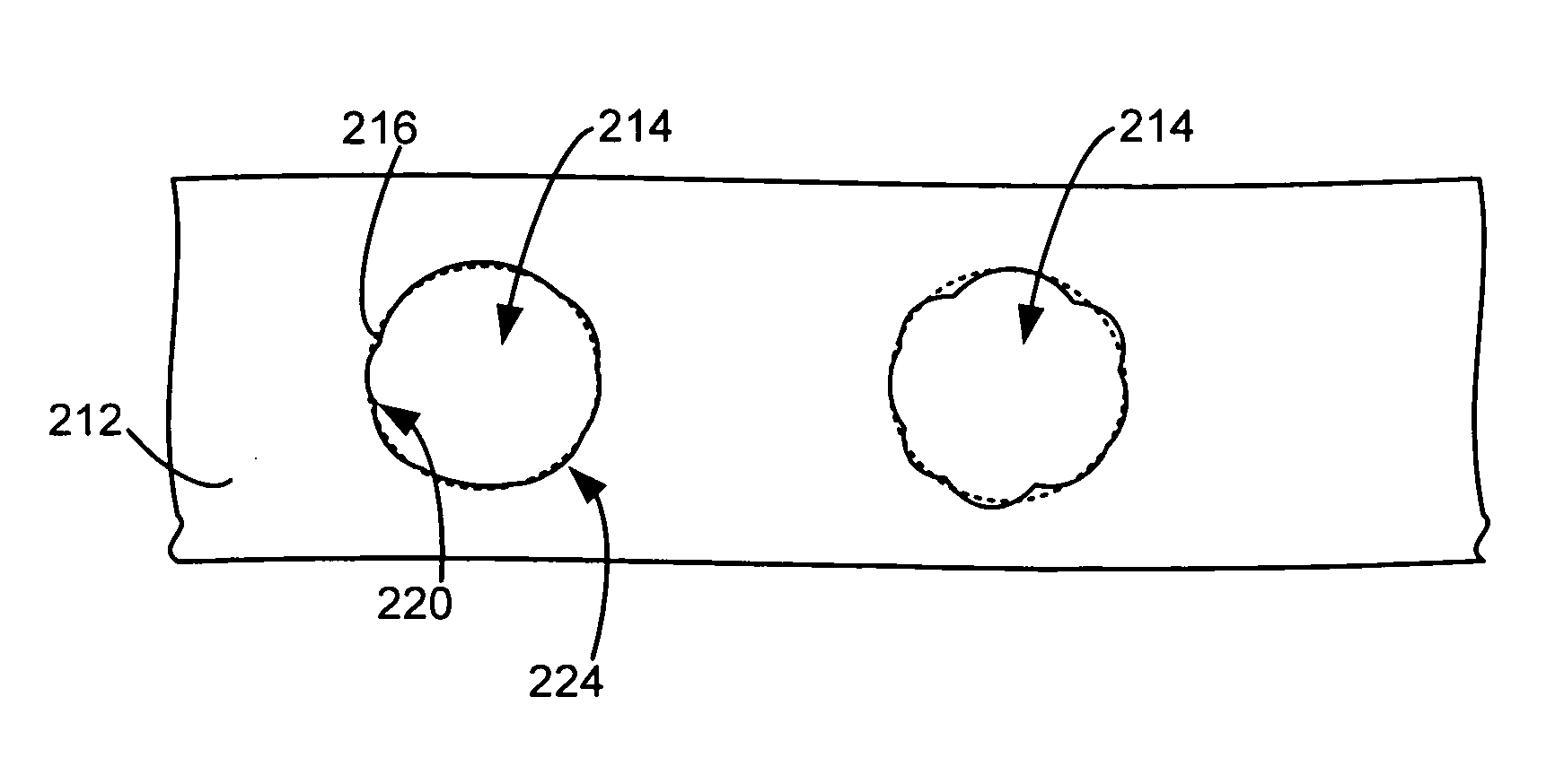
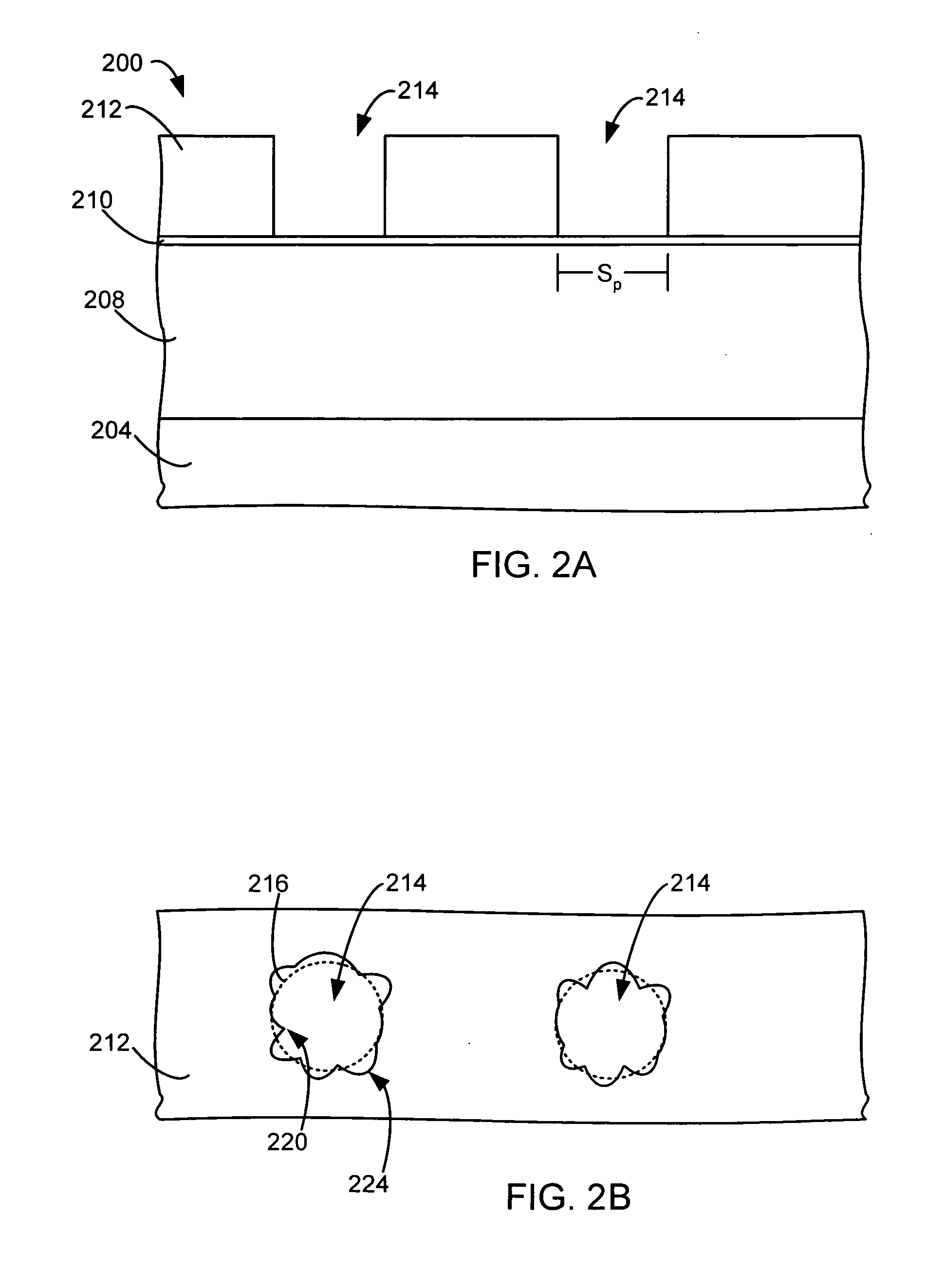
[0022] In an example of this process patterned photoresist layer is formed (step 104). A substrate 204, with the etch layer 208, an ARC layer 210, and a patterned photoresist mask 212 is placed in an etch chamber.
[0023]FIG. 4 is a schematic view of an processing chamber 400 that may be used for enlarging the photoresist features, reducing striations, etching, and stripping. The plasma processing chamber 400 comprises confinement rings 402, an upper electrode 404, a lower electrode 408, a gas source 410, and an exhaust pump 420. The gas source 410 comprises a deposition gas source 412 and an etch back gas source 416. The gas source 410 may comprise additional gas sources, such as an etching gas source 418. Within plasma processing chamber 400, the substrate 204 is positioned upon the lower electrode 408. The lower electrode 408 incorporates a suitable substrate chucking mechanism (e.g., electrostatic, mechanical clamping, or the like) for holding the substrate 204. The reactor top 4...
PUM
 Abstract
Description
Claims
Application Information