Display device and manufacturing method thereof

a technology of display device and manufacturing method, which is applied in the direction of discharge tube/lamp details, discharge tube luminescnet screen, organic semiconductor device, etc., can solve the problems of significant deterioration of luminance property such as luminance or evenness of luminance, and low reliability, and achieve high reliability of display device, high-quality images, and low cost

Active Publication Date: 2006-09-14
SEMICON ENERGY LAB CO LTD
View PDF33 Cites 82 Cited by
  • Summary
  • Abstract
  • Description
  • Claims
  • Application Information

AI Technical Summary

Benefits of technology

[0017] By using the present invention, a highly reliable display device can be manufactured through a simplified process. Ther

Problems solved by technology

An EL element has a problem that a luminance property such as luminance or evenness of luminance significantly deteriorates as compa

Method used


Image

  • Display device and manufacturing method thereof
  • Display device and manufacturing method thereof
  • Display device and manufacturing method thereof

Examples


embodiment mode 1

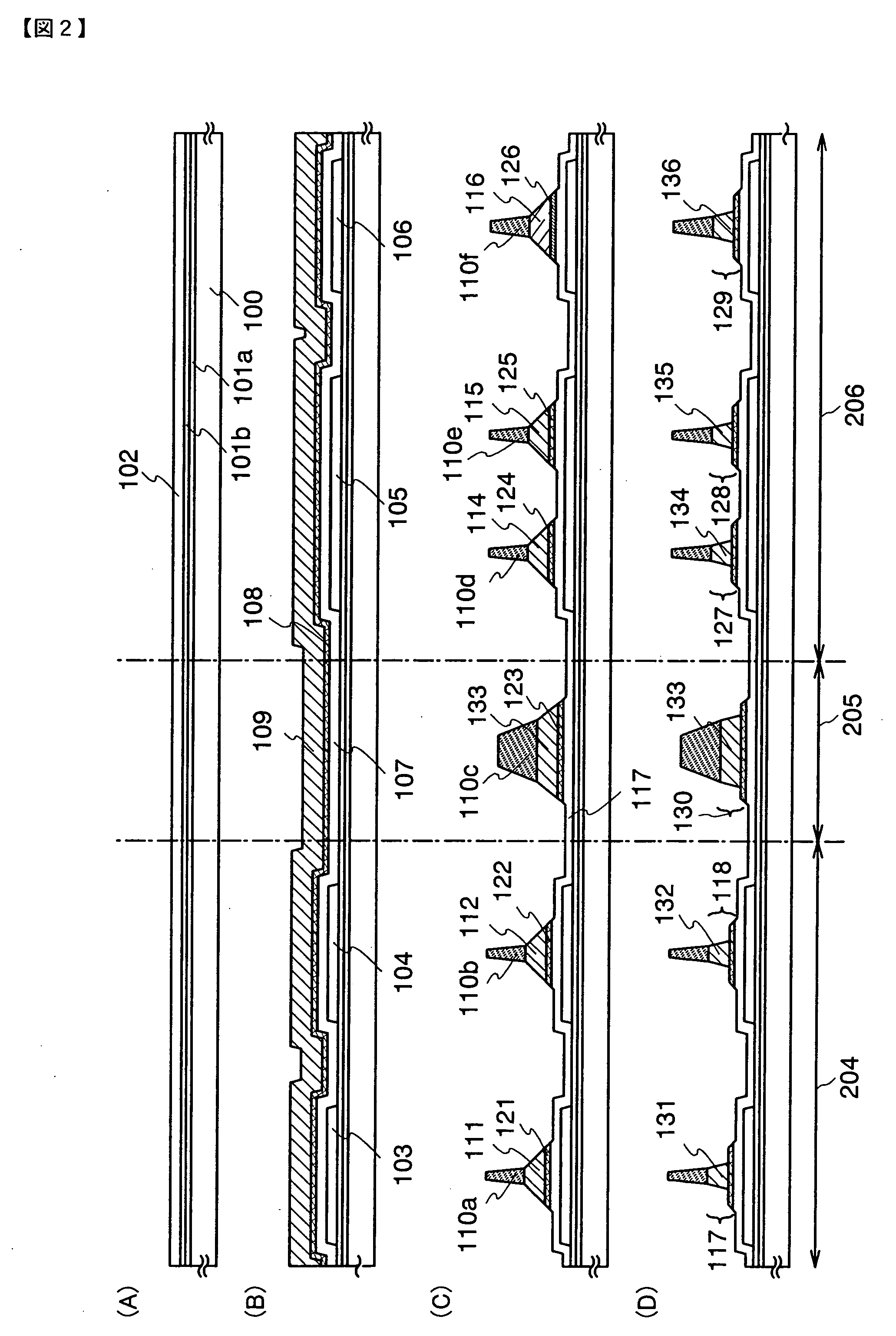
[0019] A method for manufacturing a thin film transistor in the present embodiment mode will be described in detail by using to FIG. 1 to FIG. 3.

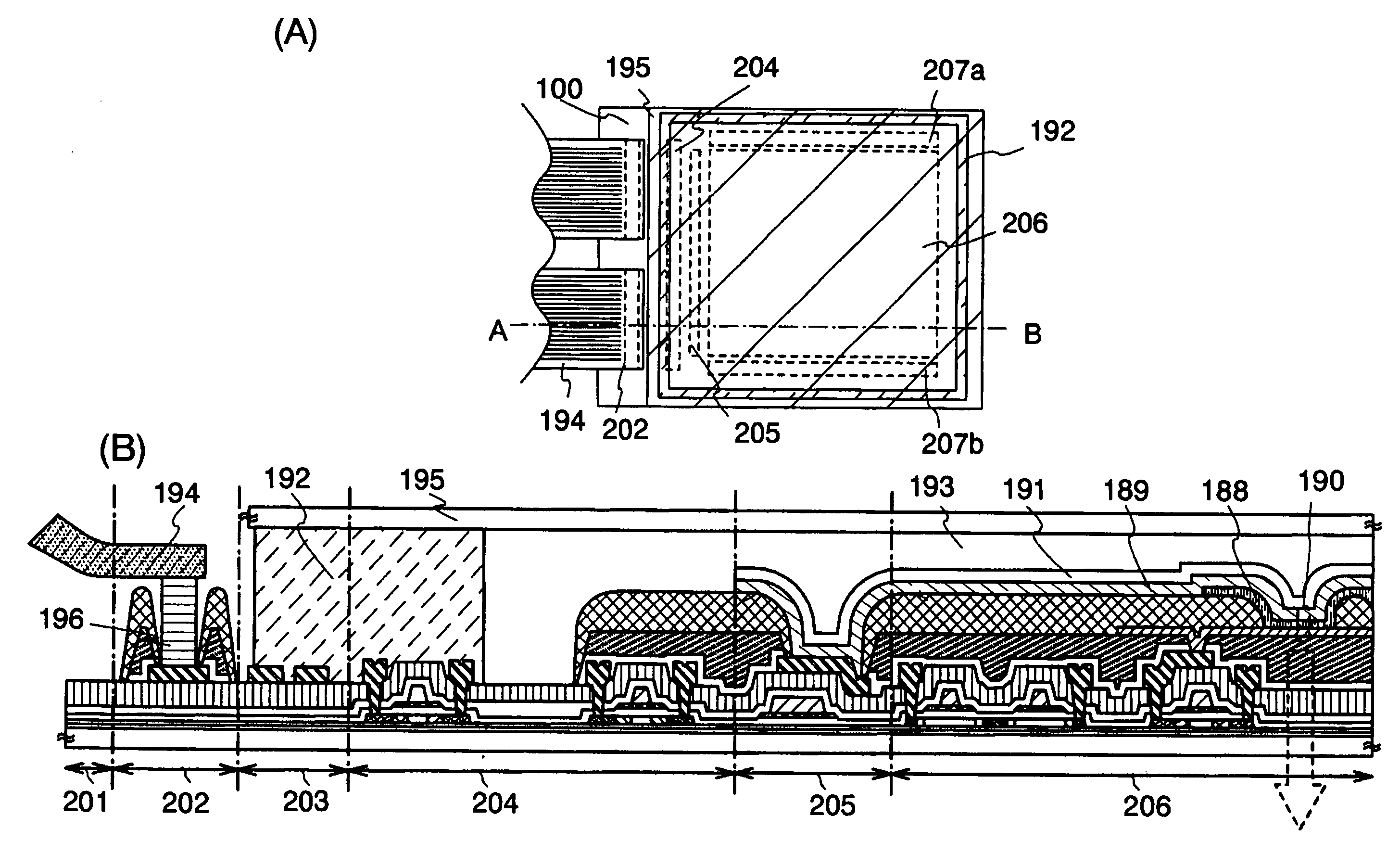
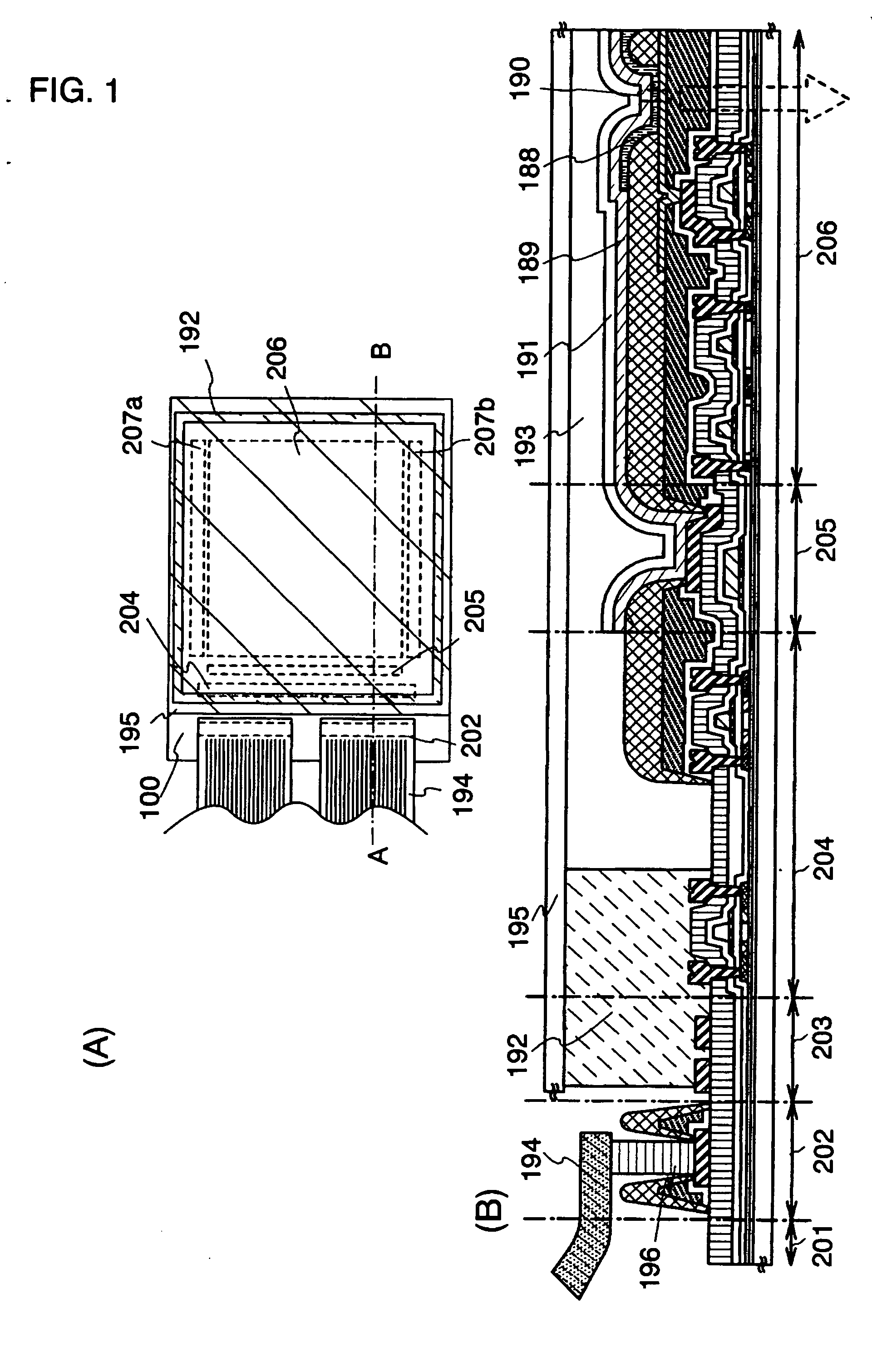
[0020]FIG. 16(A) is a top view that illustrates a structure of a display panel relating to the present invention. A pixel portion 2701 in which pixels 2702 are arranged over a matrix, a scanning line input terminal 2703, and a signal line input terminal 2704 are formed over a substrate 2700 that has an insulating surface. The number of pixels may be provided depending on various standards, and the number may be 1024×768×3 (RGB) in XGA, 1600×1200×3 (RGB) in UXGA, and 1920×1080×3 (RGB) in order to be ready for a full-speck high vision.

[0021] The pixels 2702 are arranged in a matrix by crossing a scanning line extended from the scanning line input terminal 2703 and a signal line extended from the signal line input terminal 2704. Each of the pixels 2702 is provided with a switching element and a pixel electrode layer connected thereto. A typi...

embodiment mode 2

[0125] Embodiment Mode of the present invention will be described with reference to FIG. 7 to FIG. 9. The present embodiment mode describes an example in which a second interlayer insulating layer is not formed in the display device manufactured in Embodiment Mode 1. Therefore, the repeated description of the same portions and the portions that has the same function is omitted.

[0126] As described in Embodiment Mode 1, a thin film transistor 173, a thin film transistor 174, a thin film transistor 175, a thin film transistor 176, a conductive layer 177, an insulating film 168 and an insulating film 168 are formed over a substrate 100. A source electrode layer or drain electrode layer connected to a source region or drain region of a semiconductor layer is formed in each thin film transistor. A first electrode layer 395 is formed to be in contact with a source electrode layer or drain electrode layer 172b in the thin film transistor 176 provided in a pixel region 206 (refer to FIG. 7(...

embodiment mode 3

[0131] Embodiment Mode of the present invention will be described with reference to FIG. 10. The present embodiment mode describes an example in which a gate electrode layer of a thin film transistor has a different structure in the display device manufactured in Embodiment Mode 1. Therefore, the repeated description of the same portions and the portions that has the same function is omitted.

[0132] FIGS. 10(A) to (C) show a display device that is in a manufacturing process and corresponds to the display device shown in FIG. 4(B) described in Embodiment Mode 1.

[0133] In FIG. 10(A), a thin film transistor 273 and a thin film transistor 274 are formed in a peripheral driver circuit region 214; a conductive layer 277 is formed in a connection region 215; and a thin film transistor 275 and a thin film transistor 276 are formed in a pixel region 216. A gate electrode layer of a thin film transistor in FIG. 10(A) has a stacked structure of two conductive films, in which an upper gate ele...


PUM


Abstract

It is an object of the present invention to provide a technology for manufacturing a highly reliable display device at a low cost with high yield. In the present invention, a spacer is formed over a pixel electrode, thereby protecting the pixel electrode layer from a mask in formation of an electroluminescent layer. In addition, since a layer that includes an organic material that has water permeability is sealed in a display device with a sealing material and the sealing material and the layer that includes the organic material are not in contact, deterioration of a light-emitting element due to a contaminant such as water can be prevented. The sealing material is formed in a portion of a driver circuit region in the display device, and thus, the narrower frame margin of the display device can also be accomplished.

Description

TECHNICAL FIELD [0001] The present invention relates to a display device and a method for manufacturing the display device. BACKGROUND ART [0002] An EL element has a problem that a luminance property such as luminance or evenness of luminance significantly deteriorates as compared with the beginning when it is driven for a certain period. This low reliability is a factor in the limited practical application. [0003] As one factor of worsening reliability, water, oxygen or the like which enters into the EL element from outside is given. [0004] Development of a display device that has a structure for preventing the deterioration of the EL element has been conducted. In addition, there is also a method by which a sealing material is formed over an insulator provided with an EL element, and an enclosed space surrounded by a covering material and the sealing material is filled with a filler composed of a resin or the like with the use of the sealing material so that the EL element is bloc...

Claims


Application Information

Patent Timeline
IPC IPC(8): H01J1/62H05B44/00
CPCH01L27/3244H01L27/3295H01L27/3297H01L51/0005H01L51/5237H01L51/56H01L2251/5323H10K59/122H10K71/135H10K59/12H10K59/131H10K50/8428H10K2102/3031H10K71/00H05B33/04H05B33/10H05B33/22H10K59/123H10K59/1213H10K59/125H10K59/126H10K50/13H10K50/84H10K50/11H10K50/805H10K50/844H10K50/8426H10K59/00
Inventor MURAKAMI, SATOSHIOHTANI, HISASHIYAMAZAKI, SHUNPEI
Owner SEMICON ENERGY LAB CO LTD
Why Eureka
Try Eureka