Technique for the growth of planar semi-polar gallium nitride

a gallium nitride and semi-polar technology, applied in the direction of polycrystalline material growth, crystal growth process, chemically reactive gas growth, etc., can solve the undesirable qcse, red-shifted emission, restricted carrier recombination efficiency, etc., to reduce the polarization effect of würtzite-structure iii-nitride device structur

Active Publication Date: 2006-09-14
JAPAN SCI & TECH CORP
View PDF8 Cites 242 Cited by
  • Summary
  • Abstract
  • Description
  • Claims
  • Application Information

AI Technical Summary

Benefits of technology

[0033] The present invention describes a method for growing semi-polar nitrides as planar films, such as {10{overscore (1)}1}, {10{overscore (1)}3}, and {11{overscore (2)}2} planar films of GaN. Growth of semi-polar nitride semiconductors offer a means of reducing polarization effects in würtzite-structure III-nitride device structures.

Problems solved by technology

However, conventional c-plane quantum well structures in III-nitride based optoelectronic and electronic devices suffer from the undesirable quantum-confined Stark effect (QCSE), due to the existence of strong piezoelectric and spontaneous polarizations.
The strong built-in electric fields along the c-direction cause spatial separation of electrons and holes that in turn give rise to restricted carrier recombination efficiency, reduced oscillator strength, and red-shifted emission.
Unfortunately, despite advances made by researchers at the University of California, for example, as described in the applications cross-referenced above, growth of non-polar GaN remains challenging and has not yet been widely adopted in the III-nitride industry.
Bulk crystals of GaN are not available, so it is not possible to simply cut a crystal to present a surface for subsequent device regrowth.
In addition, the surface area is too small to process into a semi-polar LED.
Furthermore, forming device structures on inclined facets is significantly more difficult than forming those structures on normal planes.

Method used


Image

  • Technique for the growth of planar semi-polar gallium nitride
  • Technique for the growth of planar semi-polar gallium nitride
  • Technique for the growth of planar semi-polar gallium nitride

Examples


Embodiment Construction

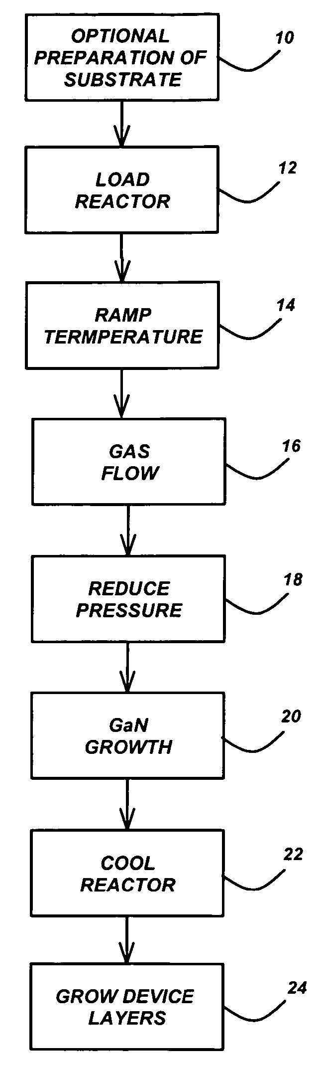
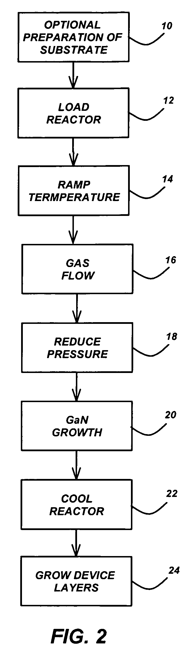
[0038] In the following description of the preferred embodiment, reference is made to the accompanying drawings which form a part hereof, and in which is shown by way of illustration a specific embodiment in which the invention may be practiced. It is to be understood that other embodiments may be utilized and structural changes may be made without departing from the scope of the present invention.

[0039] Overview

[0040] Growth of semi-polar nitride semiconductors, for example, {10{overscore (1)}1}, {10{overscore (1)}3} and {11{overscore (2)}2} planes of GaN, offer a means of reducing polarization effects in würtzite-structure III-nitride device structures. The semiconductor term nitrides refers to (Ga,Al,In,B)N and any alloy composition of these semiconductors. Current nitride devices are grown in the polar [0001] c-direction, which results in charge separation along the primary conduction direction in vertical devices. The resulting polarization fields are detrimental to the perfo...


PUM

PropertyMeasurementUnit
diameteraaaaaaaaaa
temperatureaaaaaaaaaa

Abstract

A method for growing planar, semi-polar nitride film on a miscut spinel substrate, in which a large area of the planar, semi-polar nitride film is parallel to the substrate's surface. The planar films and substrates are: (1) {10{overscore (1)}1} gallium nitride (GaN) grown on a {100} spinel substrate miscut in specific directions, (2) {10{overscore (1)}3} gallium nitride (GaN) grown on a {110} spinel substrate, (3) {11{overscore (2)}2} gallium nitride (GaN) grown on a {1{overscore (1)}00} sapphire substrate, and (4) {11{overscore (1)}3} gallium nitride (GaN) grown on a {1{overscore (1)}00} sapphire substrate

Description

CROSS-REFERENCE TO RELATED APPLICATIONS [0001] This application claims the benefit under 35 U.S.C. Section 119(e) of the following co-pending and commonly-assigned U.S. patent application: [0002] U.S. Provisional Patent Application Ser. No. 60 / 660,283, filed on Mar. 10, 2005, by Troy J. Baker, Benjamin A. Haskell, Paul T. Fini, Steven P. DenBaars, James S. Speck, and Shuji Nakamura, entitled “TECHNIQUE FOR THE GROWTH OF PLANAR SEMI-POLAR GALLIUM NITRIDE,” attorneys' docket no. 30794.128-US-P1; [0003] which application is incorporated by reference herein. [0004] This application is related to the following co-pending and commonly-assigned applications: [0005] U.S. Provisional Patent Application Ser. No. 60 / 686,244, filed on Jun. 1, 2005, by Robert M. Farrell, Troy J. Baker, Arpan Chakraborty, Benjamin A. Haskell, P. Morgan Pattison, Rajat Sharma, Umesh K. Mishra, Steven P. DenBaars, James S. Speck, and Shuji Nakamura, entitled “TECHNIQUE FOR THE GROWTH AND FABRICATION OF SEMIPOLAR (G...

Claims


Application Information

Patent Timeline
Patent Type & Authority Applications(United States)
IPC IPC(8): H01L21/28H01L21/3205H01L33/00
CPCC30B25/02C30B25/18C30B29/406H01L21/0242Y10S438/938H01L21/0254H01L21/02658H01L33/007H01L21/02433H01L21/20
Inventor BAKER, TROY J.HASKELL, BENJAMIN A.FINI, PAUL T.DENBAARS, STEVEN P.SPECK, JAMES S.NAKAMURA, SHUJI
Owner JAPAN SCI & TECH CORP
Why Eureka
Try Eureka