Electrophoretic display device and driving method thereof

Active Publication Date: 2006-09-21
E INK CORPORATION
View PDF10 Cites 58 Cited by
  • Summary
  • Abstract
  • Description
  • Claims
  • Application Information

AI Technical Summary

Benefits of technology

[0007] An advantage of the invention is to provide an electrophoretic display device in which the persistence of the image and the contrast deterioration are prevented and improved and to provide a display method thereof.
[0008] According to first aspect of the invention, an electrophoretic display device includes a first substrate, a second substrate, an electrophoretic material interposed between the first substrate and the second substrate, the electrophoretic material including a positively charged particle and a negatively charged particle, a common electrode provided on the second substrate, a pixel provided at an intersection of a signal line and a scan line, the pixel provided in a plural number and arranged in matrix on the first substrate. The electrophoretic display device further includes a pixel electrode provided in the pixel, a capacitor line provided in the pixel, a storage capacitor provided in the pixel, and a second electrode of the storage capacitor being coupled to a storage capacitor line and a thin film transistor (TFT) provided in the pixel, a source electrode of the TFT being coupled to a first electrode of the storage capacitor and the pixel electrode, a drain electrode of the TFT being coupled to the signal line, and a gate electrode of the TFT being coupled to the scan line. A capacitor line low select signal VSL or a capacitor line non-select signal VSC having a higher electric potential than an electric potential of the capacitor line low select signal VSL is supplied to the storage capacitor line.
[0009] In this way, the electric field between the pixel electrode and the common electrode is externally set by controlling high and low (level) of the electric potential of the storage capacitor line. Accordingly, it is possible to prevent a luminance level shift and the contrast deterioration after the image data writing.
[0010] According to a second aspect of the invention, an electrophoretic display device includes a first substrate, a second substrate, an electrophoretic material interposed between the first substrate and the second substrate, the electrophoretic material including a positively charged particle and a negatively charged particle, a common electrode provided on the second substrate, a pixel provided at an intersection of a signal line and a scan line, the pixel provided in a plural number and a

Problems solved by technology

When the image displayed by the electrophoretic display device is reset and a new image is formed, the reset is sometimes carried out insufficiently depending on the state of the displayed image before the reset, producing an afterimage which is persistence of a part of the image p

Method used


Image

  • Electrophoretic display device and driving method thereof
  • Electrophoretic display device and driving method thereof
  • Electrophoretic display device and driving method thereof

Examples


specific examples

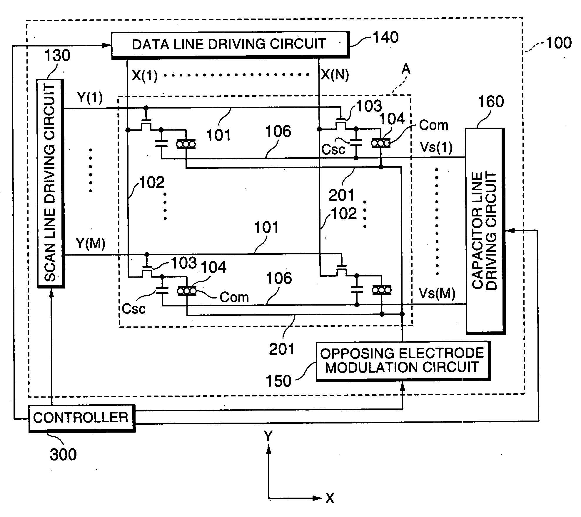
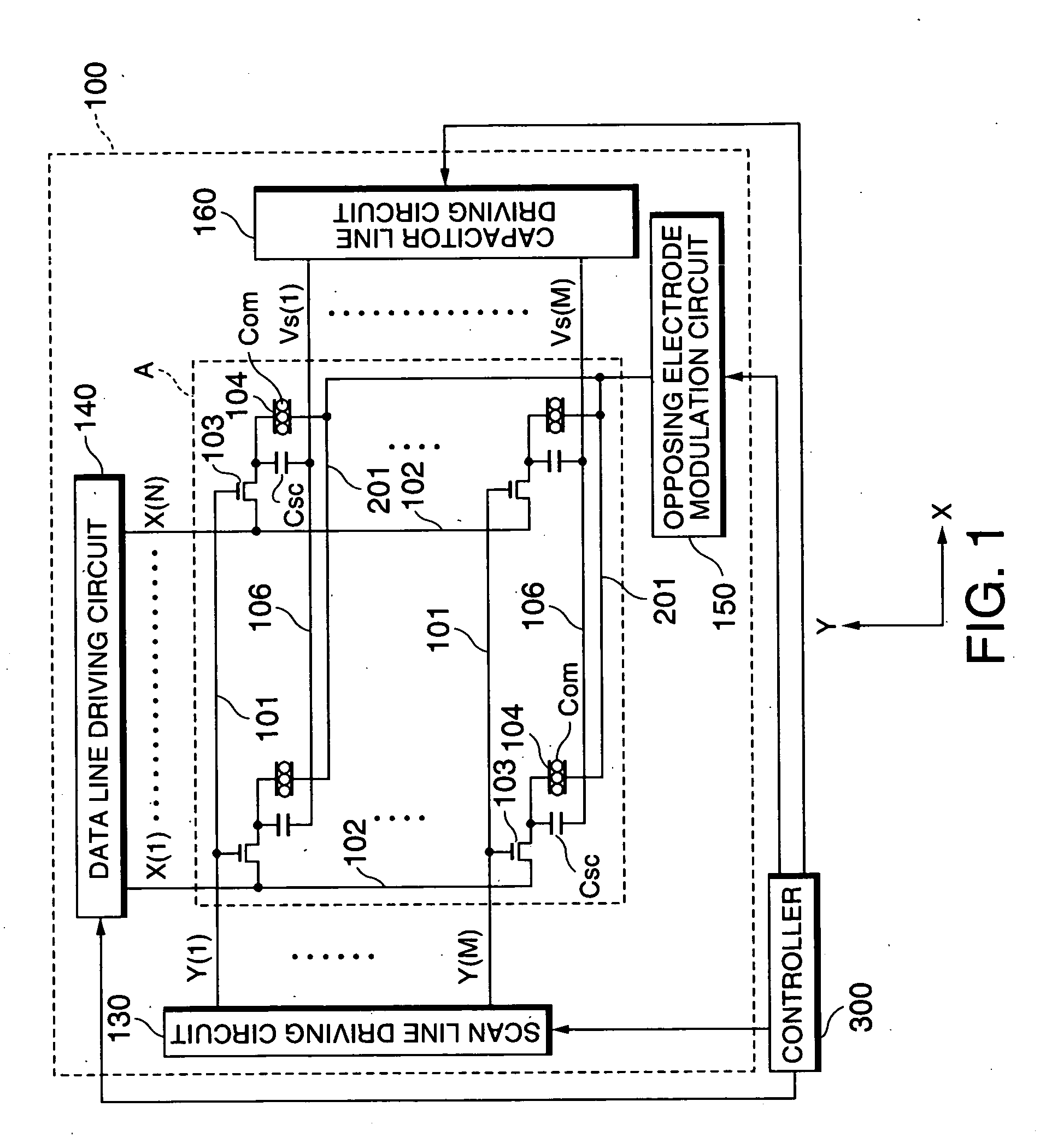
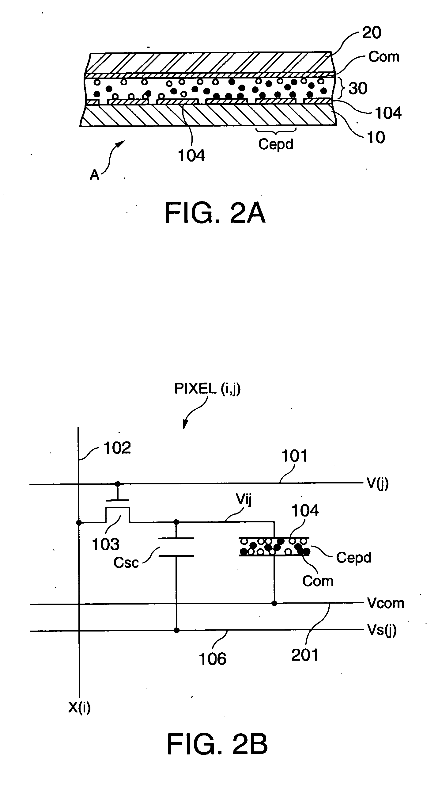
[0155]FIGS. 6 through 9 schematically show the states of the electric field between the common electrode and the pixel electrode and the states of the electrophoretic particle in the above described embodiment according to various display conditions. In FIGS. 6 through 9, Fig. A shows a state of a previous screen, Fig. B shows a state of the negatively charged white particle reset, Fig. C shows the standby state, Fig. D shows the writing state and Fig. E shows the data hold state. In the figures, the upper electrode is the common electrode Com and the lower electrode is the pixel electrode. Voltage of each electrode and the voltage values used in the above described embodiments are also shown in the figures. The voltage of the pixel electrode in the pixel (i, j) is denoted as Vij.

[0156]FIG. 6 shows the case where the negatively charged particle reset is performed when the pixel of the previous screen is black and the white writing is then carried out. If the negatively charged part...


PUM


Abstract

An electrophoretic display device including a first substrate, a second substrate, an electrophoretic material interposed between the first substrate and the second substrate, the electrophoretic material including a positively charged particle and a negatively charged particle, a common electrode provided on the second substrate, a pixel provided at an intersection of a signal line and a scan line, the pixel provided in a plural number and arranged in matrix on the first substrate. The electrophoretic display device further including a pixel electrode provided in the pixel, a capacitor line provided in the pixel, a storage capacitor provided in the pixel, and a second electrode of the storage capacitor being coupled to a storage capacitor line and a thin film transistor (TFT) provided in the pixel, a source electrode of the TFT being coupled to a first electrode of the storage capacitor and the pixel electrode, a drain electrode of the TFT being coupled to the signal line, and a gate electrode of the TFT being coupled to the scan line. A capacitor line low select signal VSL or a capacitor line non-select signal VSC having a higher electric potential than an electric potential of the capacitor line low select signal VSL is supplied to the storage capacitor line.

Description

BACKGROUND OF THE INVENTION [0001] 1. Technical Field [0002] The present invention relates to improve an electrophoretic display device. [0003] 2. Related Art [0004] An electrophoretic display device has an element substrate on which a plurality of pixel electrodes are formed, an opposing substrate that is provided so as to oppose the element substrate, and an electrophoretic layer placed between these substrates. A common electrode is formed on a face of the opposing substrate opposing to the element substrate. The electrophoretic layer is made of a dispersion medium and more than one kind of charged electrophoretic particles dispersed in the dispersion medium. [0005] JP-A-2004-94168 and JP-A-2004-157450 are examples of related art. As described in the examples, when an electric potential difference is given between the common electrode and the pixel electrode, the charged electrophoretic particle is drawn to either one of the electrodes depending on the direction of the electric f...

Claims


Application Information

Patent Timeline
IPC IPC(8): G09G3/34
CPCG09G3/344G09G2300/0876G09G2320/066
Inventor MIYASAKA, MITSUTOSHI
Owner E INK CORPORATION
Why Eureka
Try Eureka