Demodulation circuit for use in receiver using if directing sampling scheme

Inactive Publication Date: 2006-09-21
SAMSUNG ELECTRONICS CO LTD
11 Cites 5 Cited by

AI-Extracted Technical Summary

Problems solved by technology

Therefore, the receiver is disadvantageous in that it has a large hardware size because it needs pairs of the mixers and the LPFs, and the cost is ...

Benefits of technology

[0018] A feature of the present invention is to provide a demodulation circuit for...

Abstract

Disclosed is a demodulation circuit for demodulating an IF signal which is input via an antennal and then over-sampled at a sampling rate four times a frequency of a baseband signal, the demodulation circuit including a mixer for converting the IF signal down to a baseband signal using a coefficient corresponding to either sine values or cosine values, a DEMUX for dividing the down-converted baseband signal into a plurality of signals, and a PPF having a plurality of sub-filters for filtering the divided signals input from the DEMUX and a plurality of adders for operating the output signals of the sub-filters. As a result, the demodulation circuit can be realized in a small hardware size and is capable of reducing power consumption.

Application Domain

Technology Topic

Image

  • Demodulation circuit for use in receiver using if directing sampling scheme
  • Demodulation circuit for use in receiver using if directing sampling scheme
  • Demodulation circuit for use in receiver using if directing sampling scheme

Examples

  • Experimental program(1)

Example

[0029] Certain embodiments of the present invention will be described in greater detail with reference to the accompanying drawings.
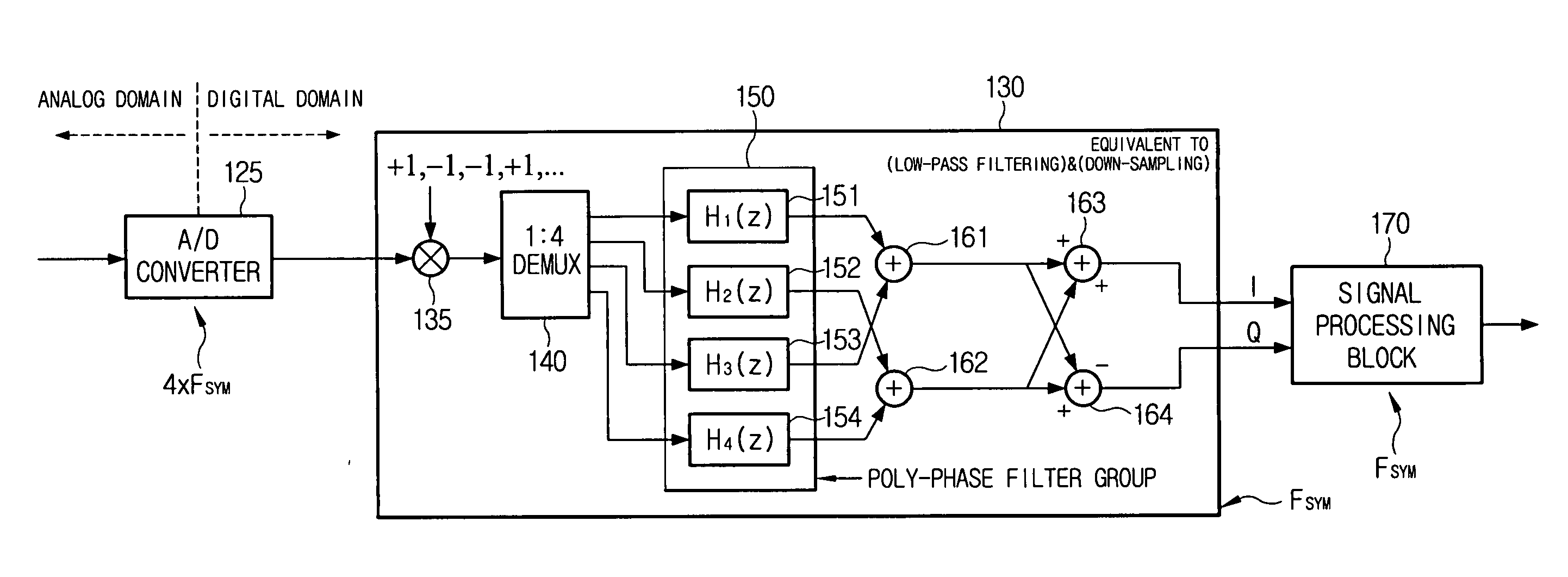
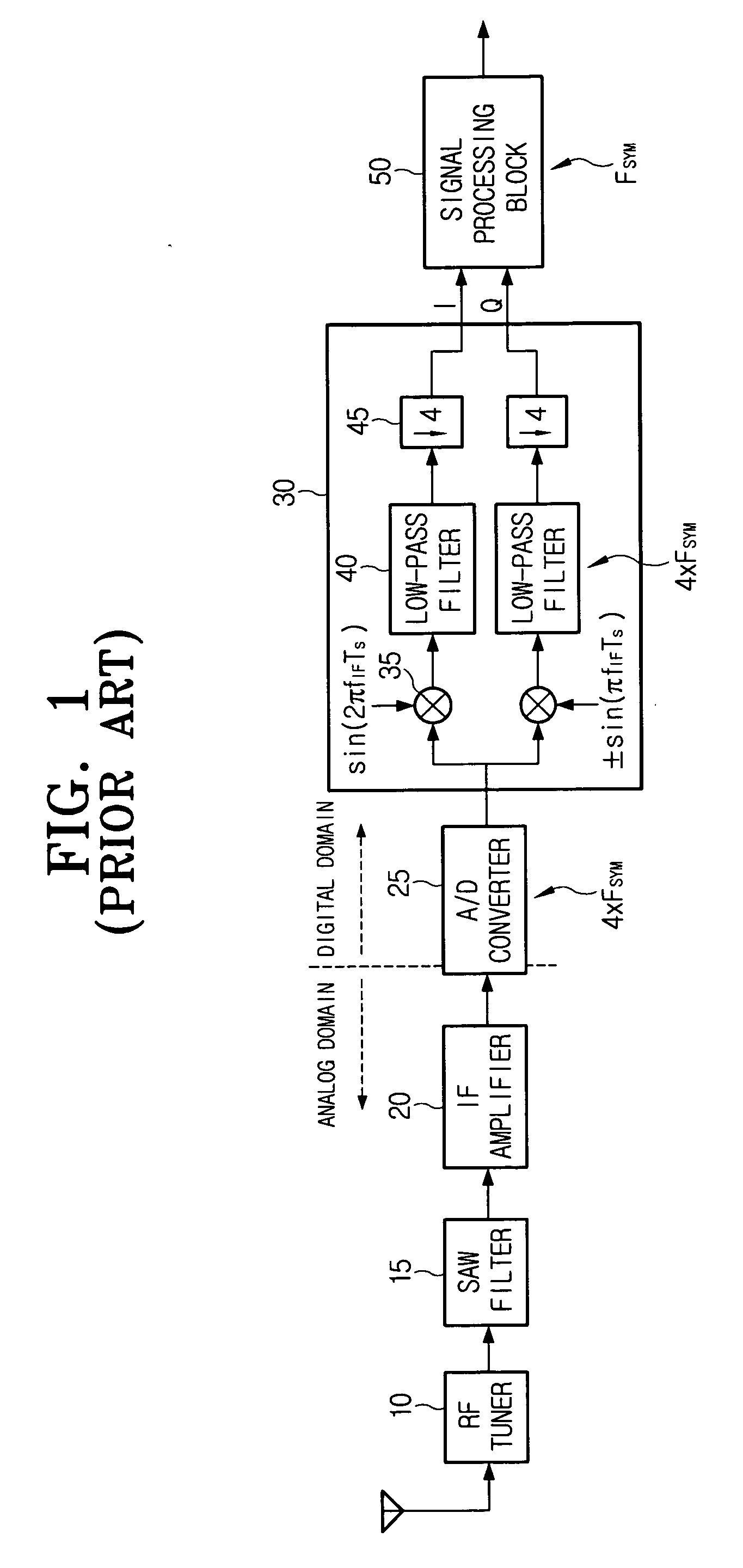
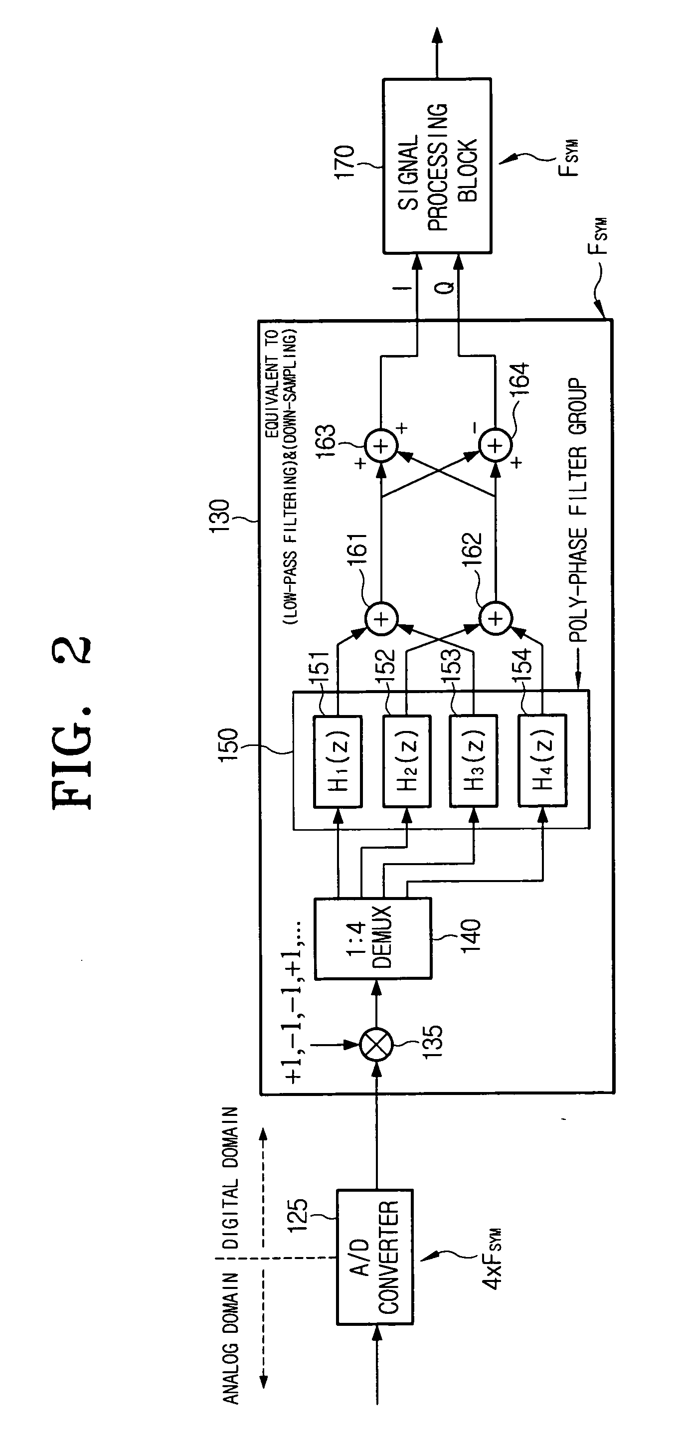
[0030] In a general receiver using an IF direct sampling scheme, an A/D converter simply digitizes an IF signal and provides the digitized IF signal to a demodulation circuit. Meanwhile, an A/D converter in a demodulation circuit in accordance with the present invention not only digitizes an IF signal but also provides a digitized signal in response to a clock signal at a frequency four times a frequency of a baseband signal to a demodulation circuit.
[0031]FIG. 2 illustrates a block diagram of a demodulation circuit for use in a receiver using an IF direct sampling scheme, in accordance with one embodiment of the present invention.
[0032] A demodulation circuit 130 includes a mixer 135, a DEMUX 140, a polyphase filter (PPF) 150, and an LPF comprised of a plurality of adders.
[0033] The mixer 135 receives a coefficient corresponding to the sine values or the cosine values from a local oscillator, and performs down-conversion with respect to an IF signal sampled by an A/D converter 125 at a sampling rate four times a frequency of an incoming using the given coefficient to a baseband signal. At this time, the coefficient for use in the down-conversion is expressed as follows since a sine wave used for the down-conversion has a frequency equal to a quarter of an incoming signal frequency:
[0034] values of a cosine wave: 0.7071×(+1, −1, −1, +1, +1, −1, −1, +1, . . . )
[0035] values of a sine wave: 0.7071×(−1, −1, +1, +1, −1, −1, +1, +1, . . . )
[0036] Here, even-numbered values of the cosine wave and the sine wave are the same but odd-numbered values of the cosine wave and the sine wave are in the opposite phase. However, such relationship between the cosine values and the sine values can be inverted by a modulation provided in a receiver.
[0037] Meanwhile, a signal output from the mixer 135 is divided into four signals by a DEMUX 140, and then the output signals of the DEMUX 140 are input to the one PPF 150. Then, the PPF 150 processes the four incoming signals using adders, thereby generating an I signal and a Q signal. Since this receiver includes only one mixer 135, the mixer 135 receives the coefficient corresponding to the values of either the cosine wave or the sine wave. That is, the mixer can receive the coefficient corresponding to the cosine values having a pattern constituted by repeating the values in order of “+1, −1, −1, +1”, or receive the coefficient corresponding to the sine values having a pattern constituted by repeating the values in order of “−1, −1, +1, +1”. In this embodiment, the coefficient corresponds to the cosine values.
[0038] The DEMUX 140 divides the baseband signal down-converted by the mixer 135 into four signals, and transmits them to the PPF. As a result, the respective sub-filters of the PPF 150 receive sequentially the basebadnd signals down-converted with the coefficient “+1, −1, −1, +1.”
[0039] The PPF 150 is a kind of an LPF and includes a first sub-filter 151, a second sub-filter 152, a third sub-filter 153 and a fourth sub-filter 154.
[0040] The transfer function H(z) of the PPF is defined by Equation 1 below.
H(z)=h0+h1z−1+h2z−2+h3z−3+ . . . +hN−2z−(N−2)+hN−1z−(N−1) Equation 1
[0041] To realize the first to fourth sub-filters 154, decomposition must be performed twice in the PPF 150. First-order decomposed transfer functions acquired by performing the decomposition once are expressed as in Equation 2.
Hodd(z2)=h0+h2z−2+h4z−4+ . . . +hN−2z−(N−2)
Heven(z2)=h1z−1+h3z−3+h5z−5+ . . . +hN−1z−(N−1)  Equation 2
[0042] At this time, the relationship between the transfer function H(z) of the PPF 150 and first-order decomposed transfer functions, Hodd(z2)and Heven(z2), is s follows:
H(z)=Hodd(z2)+z−1Heven(z2)
[0043] Meanwhile, in case that the first-order decomposed transfer functions, Hodd(z2) and Heven(z2), expressed in Equation 2 are decomposed, functions H1(z4), H2(z4), H3(z4), and H4(z4), which are the transfer functions of the first to the fourth sub-filters 154 and expressed in Equation 3, are acquired.
H1(z4)=h0+h4z−4+h8z−8+ . . . +hN−4z−(N−4)
H2(z4)=h1z−1+h5z−5+h9z−9+ . . . +hN−3z−(N−3)
H3(z4)=h2z−2+h6z−6+h10z−10+ . . . +hN−2z−(N−2)
H4(z4)=h3z−3+h7z−7+h11z−11+ . . . +hN−1z−(N−1) Equation 3
[0044] Here, the relationships between the first-order decomposed transfer functions and the second-order decomposed transfer functions are as follows:
Hodd(z2)=H1(z4)+z−2H3(z4)
Heven(z2)=z−1H2(z4)+z−3H4(z4)
[0045] As described above, since the PPF 150 is comprised of four sub-filters and by performing two-step decomposition processes, the clock speed can be reduced to ¼ thereof, thereby preventing the PPF 150 from operating at high speed during the processing of the samples at a frequency which is increased four times by the A/D converter 125.
[0046] At output terminals of the four sub-filters, the first to fourth adders 164 are applied, respectively. The first adder 161 and the second adder 162 processes output signals of the first to the fourth sub-filters 154, and the third adder 163 and the fourth adder 164 processes the output signals of the first and the second adders 161, 162.
[0047] The first adder 161 outputs a signal by adding the output signals of the first sub-filter 151 and the third sub-filter 153. At this time, the output signals of the first sub-filter 151 and the third sub-filter 153 have the opposite values, and the first adder 161 outputs the difference between the output signals of the first sub-filter 151 and the third sub-filter 153. The second adder 162 adds the output signals of the second and fourth sub-filters 152, 154. At this time, since the output signals of the second sub-filter 152 and the fourth sub-filter 154 have the opposite values, the second adder 162 outputs the difference between the values of both output signals of the second sub-filter 152 and the fourth sub-filter 154 in the same manner as the first adder 161.
[0048] The third adder 163 generates the I signal by adding the output signals of the first adder 161 and the second adder 162, and the fourth adder 164 generates the Q signal by subtracting the output signal of the first adder 161 from the output signal of the second adder 162.
[0049]FIG. 3 illustrates a block diagram of a demodulation circuit 130 in accordance with another embodiment of the present invention. As shown in FIG. 3, the output terminal of the fourth adder 164 in the present demodulation circuit 130 is connected to an inverter 175 and a MUX 180. The inverter 175 is connected to the output terminal of the fourth adder 164, but the output signal of the fourth adder 164 also can be connected to the MUX 180 by bypassing the inverter 175. Accordingly, the MUX 180 receives the output signal of the fourth adder 164 as well as an output signal of the inverter 175. The MUX 180 directly relays the Q signal generated by the fourth adder 164 to a signal processing block 170 in response to a control signal generated by the signal processing block in which the I signal and the Q signal generated in the demodulation circuit 130 are processed, or sends an inverted Q signal, which has the opposite value of the Q signal and is made by the inverter 175, to the signal processing block 170.
[0050] Generally, when modulating a signal in a transmitter, a signal is modulated by multiplying cosine values by negative sine values therewith. In case that, a signal is modulated by multiplying a cosine value by a positive sine value, or by multiplying a negative cosine value by a negative sine value, the negative and positive states of the I signal and the Q signal can be changed. In this case, the inverter 175 corrects the states of the I signal and the Q signal by inverting the states thereof. Accordingly, the inverter 175 and the MUX 180 can be applied to the output terminal of third adder 163 as well as the output terminal of the fourth adder 164.
[0051] Whether the Q signal output from the fourth adder 164 is directly input to the signal processing block 170 or the inverted Q signal produced as the Q signal passes through the inverter 175 is inputted to the signal processing block 170 is determined at the time when the demodulation circuit 130 is designed.
[0052] As described above, since the present demodulation circuit 130 has one PPF 150 comprised of four sub-filters and one LPF comprised of four adders, the number of LPFs and mixers 135 decreases. As a result, the hardware size and cost of the demodulation circuit 130 can be reduced and as the number of components decreases. Further, since the present demodulation circuit 130 can reduce an internal clock speed of the PPF 150 by two steps of decomposition, power consumption, which has a characteristic of increasing as the LPF operates at higher speed, is reduced.
[0053] The foregoing embodiment and advantages are merely exemplary and are not to be construed as limiting the present invention. The present teaching can be readily applied to other types of embodiments. Also, the description of the embodiments of the present invention is intended to be illustrative, and not to limit the scope of the claims, and many alternatives, modifications, and variations will be apparent to those skilled in the art.

PUM

no PUM

Description & Claims & Application Information

We can also present the details of the Description, Claims and Application information to help users get a comprehensive understanding of the technical details of the patent, such as background art, summary of invention, brief description of drawings, description of embodiments, and other original content. On the other hand, users can also determine the specific scope of protection of the technology through the list of claims; as well as understand the changes in the life cycle of the technology with the presentation of the patent timeline. Login to view more.

Similar technology patents

Novel three-axle swinging platform

ActiveCN104121929ALow powerLower frame heightMeasurement devicesDrive motorMoving parts
Owner:北京航天万鸿高科技有限公司

Trawl net with a plurality of parallel bag sets and catching method thereby

ActiveCN103478089AImprove survival rate and fresh qualityLow powerFishing netsEngineeringTrawling
Owner:ZHEJIANG OCEAN UNIV

Classification and recommendation of technical efficacy words

Why Eureka
Try Eureka