
Method and apparatus for reducing imager floating diffusion leakage

a technology of floating diffusion and imaging device, which is applied in the direction of diodes, semiconductor devices, radio frequency controlled devices, etc., can solve the problems of poor signal to noise ratio, inability to fully store at a floating diffusion region all the charge generated by a photosensor, and the floating diffusion region typically loses some charge transfer, etc., to achieve the effect of reducing floating diffusion leakag

Active Publication Date: 2006-09-28
MICRON TECH INC
View PDF9 Cites 27 Cited by
  • Summary
  • Abstract
  • Description
  • Claims
  • Application Information

AI Technical Summary

Benefits of technology

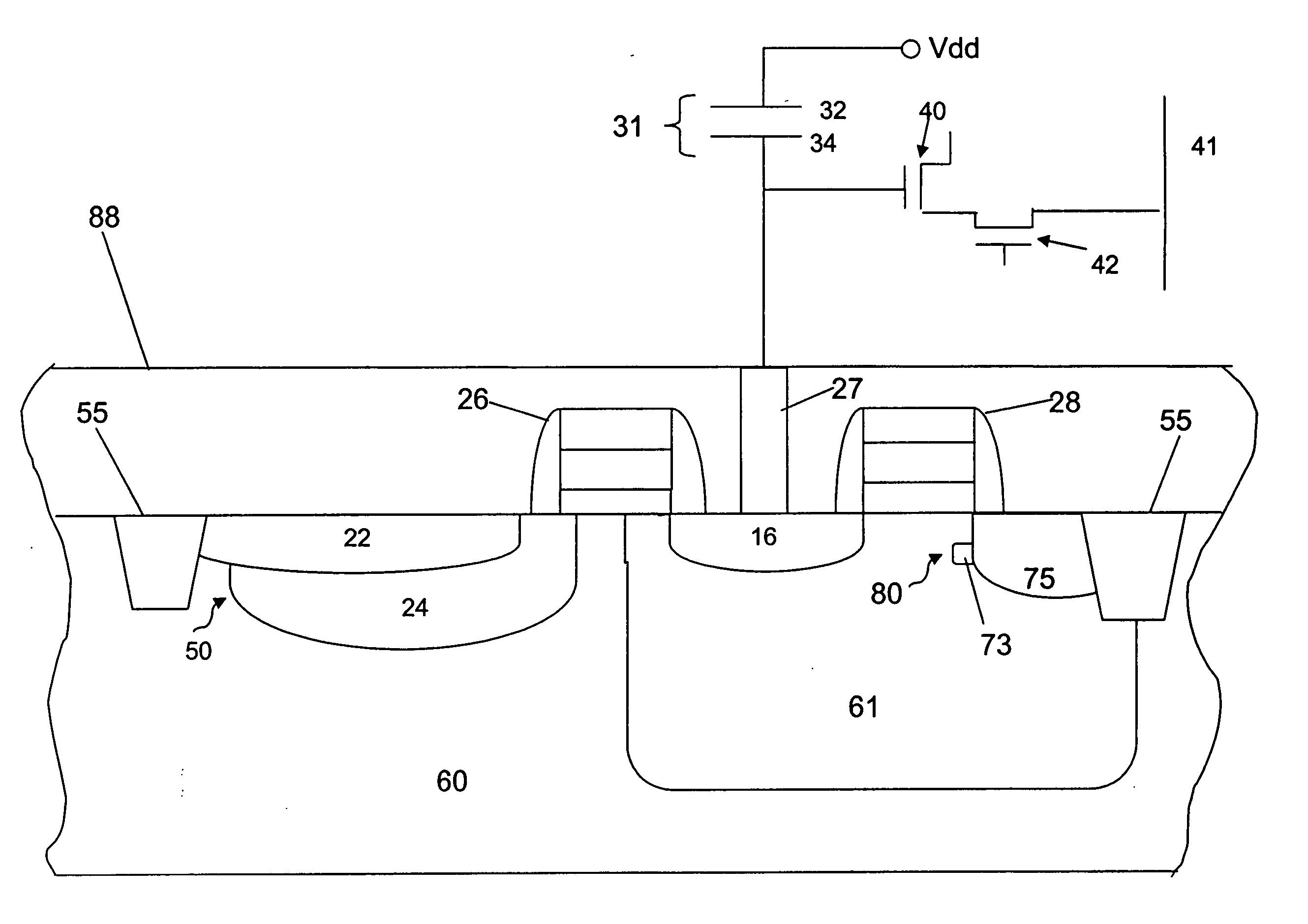
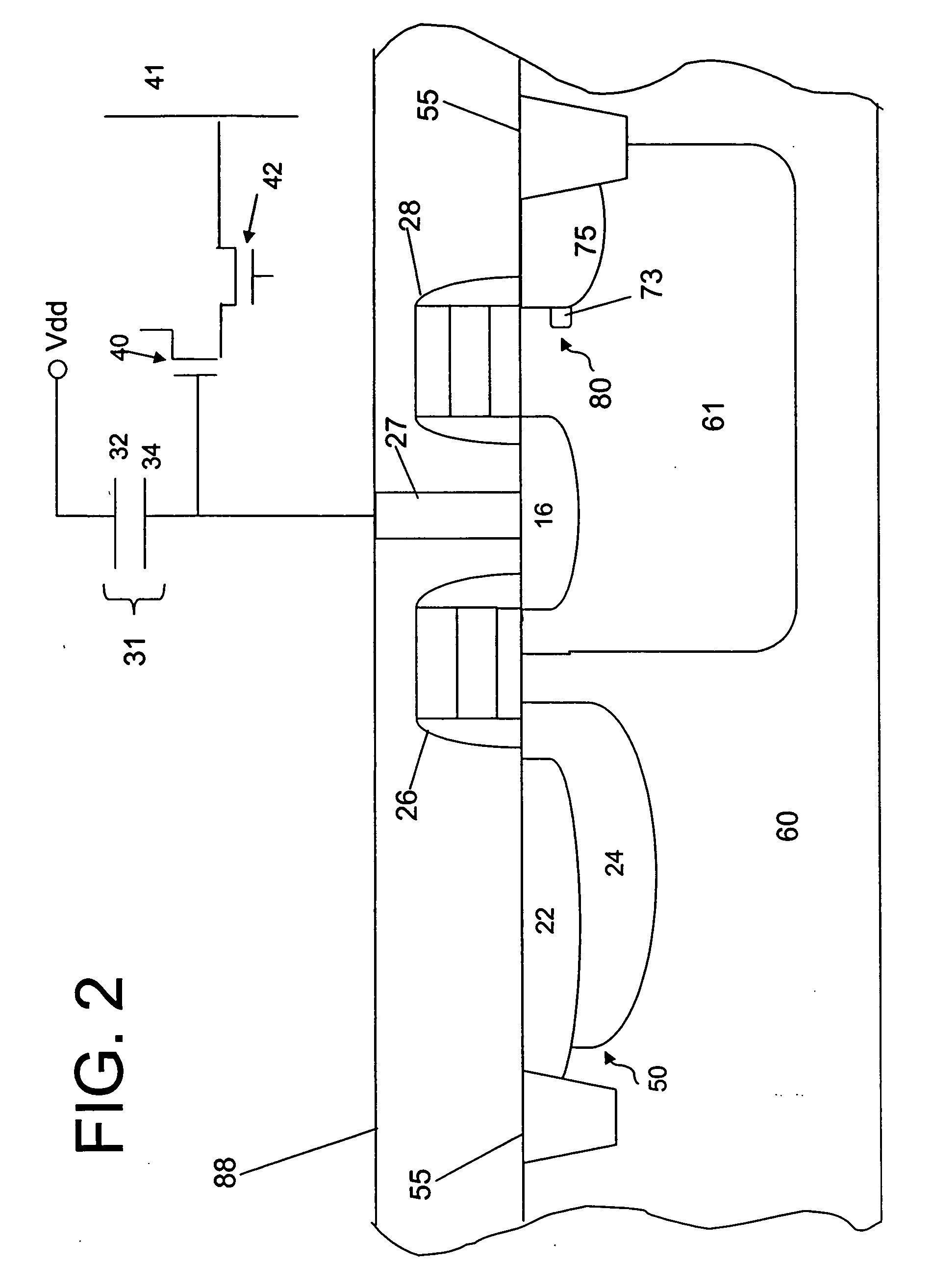
[0007] Embodiments of the present invention provide an imager having reduced floating diffusion leakage. A polysilicon contact is provided between a floating diffusion region and a gate of a source follower output transistor, with the contact also electrically connected to a storage capacitor. The storage capacitor provides additional charge storage capacity to the floating diffusion region. In addition, an associated reset transistor has different dopant characteristics in the source and drain regions. The floating diffusion region may be used in the pixels of a CMOS imager or in the output stage of a CCD imager.

Problems solved by technology

One problem associated with imagers is the inability to fully store at a floating diffusion region all charge generated by a photosensor.
In addition, the floating diffusion region typically loses some charge transferred to it.
Such charge leakage can lead to poor signal to noise ratios, punch-through at a reset transistor gate used to reset the floating diffusion region to a known state prior to a charge transfer and poor dynamic range.

Method used


Image

  • Method and apparatus for reducing imager floating diffusion leakage
  • Method and apparatus for reducing imager floating diffusion leakage
  • Method and apparatus for reducing imager floating diffusion leakage

Examples


Embodiment Construction

[0027] In the following detailed description, reference is made to the accompanying drawings, which form a part hereof and show by way of illustration specific embodiments in which the invention may be practiced. These embodiments are described in sufficient detail to enable those skilled in the art to practice the invention, and it is to be understood that other embodiments may be utilized, and that structural, logical, and electrical changes may be made without departing from the spirit and scope of the present invention. Additionally, processing steps described and their progression are exemplary of preferred embodiments of the invention; however, the sequence of steps is not limited to that set forth herein and may be changed as is know in the art, with the exception of steps necessarily occurring in a certain order.

[0028] The terms “wafer” and “substrate,” as used herein, are to be understood as including silicon, silicon-on-insulator (SOI) or silicon-on-sapphire (SOS) technol...


PUM


Abstract

An imager having reduced floating diffusion leakage and a mechanism for improving the storing of collected charge is described. A polysilicon contact is provided between a floating diffusion region and a gate of a source follower output transistor, with the contact also electrically connected to a storage capacitor. The storage capacitor provides additional charge storage capacity to the floating diffusion region. In addition, an associated reset transistor has different dopant characteristics in the source and drain regions. The floating diffusion region may be used in the pixels of a CMOS imager or in the output stage of a CCD imager.

Description

FIELD OF THE INVENTION [0001] The invention relates generally to a method and apparatus for reducing charge leakage in an imaging device. BACKGROUND OF THE INVENTION [0002] Typically, a digital imager circuit includes a focal plane array of pixel cells, each one of the cells including a photoconversion device, e.g. a photogate, a photoconductor, or a photodiode. In a CMOS imager, a readout circuit connected to each pixel cell typically includes at least an output transistor. The photoconversion device converts photons to electrons which are typically transferred to a floating diffusion (FD) region, connected to the gate of a source follower output transistor. A charge transfer device can be included as well and may be a transistor for transferring charge from the photoconversion device to the floating diffusion region. Imager cells also typically have a transistor for resetting the floating diffusion region to a predetermined charge level prior to charge transference. The output of ...

Claims


Application Information

Patent Timeline
Patent Type & Authority Applications(United States)
IPC IPC(8): H01L31/113H01L27/146H01L31/0352H01L31/062
CPCH01L27/14603H01L27/14609H01L27/14643H01L27/14683H01L27/14689H01L31/0352
Inventor RHODES, HOWARD E.
Owner MICRON TECH INC
Learn More