Semiconductor device

a technology of semiconductors and transistors, applied in the direction of logic circuits, logic circuit coupling/interface arrangements, pulse techniques, etc., can solve the problems of low peak temperature of each transistor, and achieve the effect of reducing current density, reducing the peak temperature of each transistor, and extensive area

Inactive Publication Date: 2006-09-28
RENESAS ELECTRONICS CORP
View PDF11 Cites 8 Cited by
  • Summary
  • Abstract
  • Description
  • Claims
  • Application Information

AI Technical Summary

Benefits of technology

[0005] The semiconductor device according to the publication, however, still has a room for improvement in reduction in current density at the source electrode or the drain electrode of the power transistors, as well as in lowering a peak temperature of the power transistors.
[0007] In the semiconductor device thus constructed, when the first, third and fifth source / drain regions are acting as the source, the second and fourth source / drain regions act as the drain. On the contrary, when the former acts as the drain, the latter acts as the source. Under such configuration, the third source / drain region is shared by the first and second transistors. Accordingly, the first and second transistors share either of the source or drain, which allows reducing current density at the source electrode or drain electrode of each transistor. Further, heat is generated over a more extensive area during the operation than in a device where neither the source nor drain is shared, which leads to the lower peak temperature of each transistor.
[0008] Thus, the present invention provides a semiconductor device capable of reducing current density at a source electrode or a drain electrode of each transistor, and lowering the peak temperature of each transistor.

Problems solved by technology

Further, heat is generated over a more extensive area during the operation than in a device where neither the source nor drain is shared, which leads to the lower peak temperature of each transistor.

Method used


Image

  • Semiconductor device
  • Semiconductor device
  • Semiconductor device

Examples


first embodiment

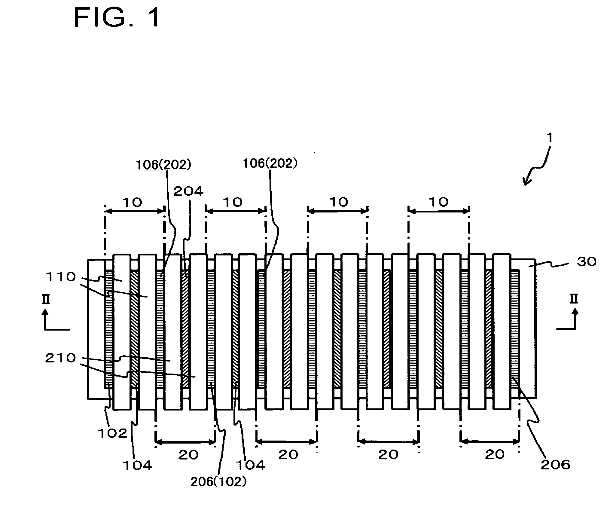
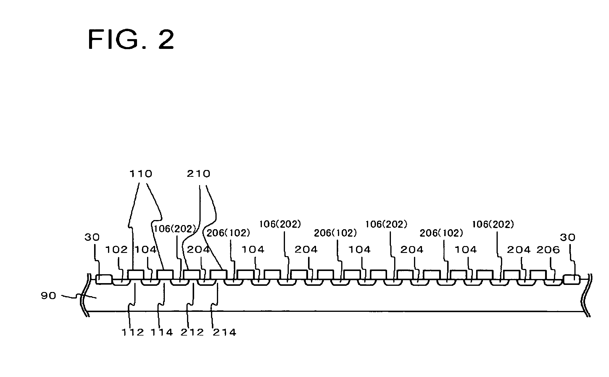
[0023]FIG. 1 is a plan view showing a semiconductor device according to the first embodiment of the present invention. FIG. 2 is a cross-sectional view taken along the line II-II of FIG. 1. The semiconductor device 1 includes transistors 10, 20.

[0024] In this embodiment, the semiconductor device 1 includes a plurality (in this case, four each) of transistors 10, 20. The transistors 10, 20 are alternately aligned in a transverse direction according to the orientation of FIG. 1. Also, as is apparent from FIG. 2, the transistors 10, 20 are located in a device-forming region surrounded by an isolation region 30 formed in a semiconductor substrate 90. Accordingly, the transistors 10 and the transistors 20 are continuously disposed in the semiconductor device 1, without being isolated by the isolation region 30. The semiconductor substrate 90 may be a silicon substrate, for example. The isolation region 30 may be a LOCOS region.

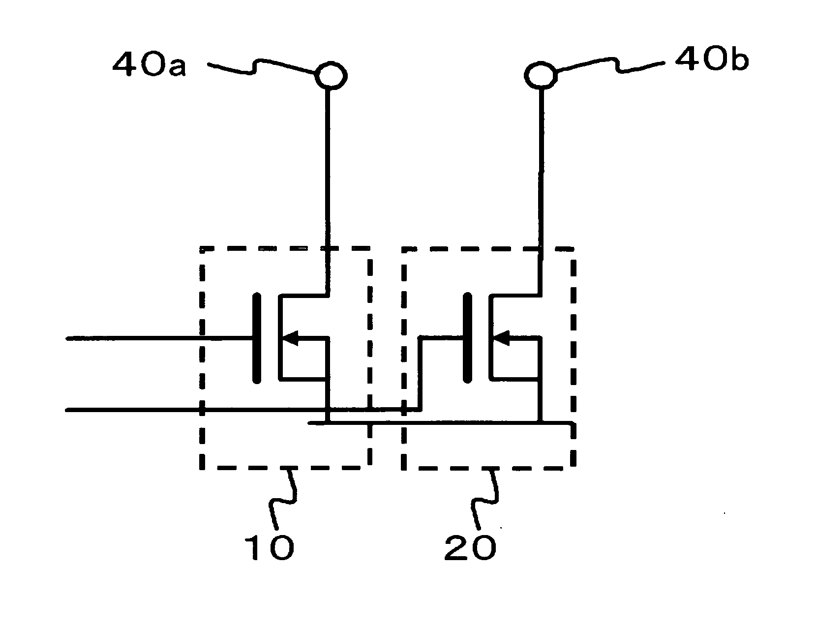
[0025] Each of the transistors 10 (first transistor) is a M...

second embodiment

[0042]FIG. 6 is a plan view showing a semiconductor device according to the second embodiment of the present invention. FIG. 7 is a cross-sectional view taken along the line VII-VII of FIG. 6. The semiconductor device 2 includes transistors 10, 20, drain interconnects 52, 54, and source interconnects 56, 58. The structure of the transistors 10, 20 is similar to that in the semiconductor device 1. In the semiconductor device 2 also, a plurality of the respective transistors 10, 20 is alternately aligned, as in the semiconductor device 1.

[0043] The drain interconnects 52, 54 and the source interconnects 56, 58 are disposed so as to extend along the alignment direction of the transistors 10, 20. These interconnects are disposed in the sequence of the source interconnect 56, the drain interconnect 52, the drain interconnect 54 and the source interconnect 58, in a direction generally orthogonal to the alignment direction. In other words, adjacent to the drain interconnect 52, the drain ...

third embodiment

[0049]FIG. 8 is a plan view showing a semiconductor device according to the third embodiment of the present invention. The semiconductor device 3 includes a plurality (in this embodiment, two) of transistor groups 70a, 70b. The structure of the transistor groups 70a, 70b is similar to that described based on FIG. 1. The transistor groups 70a, 70b are aligned in a vertical direction according to the orientation of FIG. 8. Accordingly, the transistor groups 70a, 70b are aligned generally orthogonally to the alignment direction of the transistors 10, 20 in the transistor groups 70a, 70b. The transistor group 70a and the transistor group 70b are respectively located in different device-forming regions. Therefore, the transistor group 70a and 70b are isolated from each other by the isolation region 30.

[0050] Each gate electrode of the transistor groups 70a, 70b is independently controlled from one another. More specifically, the gate electrode 110 of the transistor group 70a (first tran...


PUM


Abstract

The semiconductor device 1 includes transistors 10, 20. Each of the transistors 10 (first transistor) is a MOSFET, and includes source regions 102, 106, a drain region 104, and a gate electrode 110. Each of the transistors 20 (second transistor) is also a MOSFET, and includes source regions 202, 206, a drain region 204, and a gate electrode 210. The source region 106 of the transistor 10 and the source region 202 of the transistor 20 are the identical region in the semiconductor substrate 90. In other words, the source region 106 and the source region 202 are shared by the both transistors.

Description

BACKGROUND [0001] 1. Technical Field [0002] The present invention relates to a semiconductor device. [0003] 2. Related Art [0004] Semiconductor devices so far developed include the one disclosed in Japanese Laid-open utility model publication No. S61-51754. In the semiconductor device according to this publication, each of a plurality of regions in a single chip includes a power transistor. SUMMARY OF THE INVENTION [0005] The semiconductor device according to the publication, however, still has a room for improvement in reduction in current density at the source electrode or the drain electrode of the power transistors, as well as in lowering a peak temperature of the power transistors. [0006] According to the present invention, there is provided a semiconductor device comprising: (a) a first transistor including a first source / drain region, a second source / drain region located opposite to the first source / drain region across a first gate region, a third source / drain region located ...

Claims


Application Information

Patent Timeline
Patent Type & Authority Applications(United States)
IPC IPC(8): H03K19/094
CPCH01L21/823425H01L27/088
Inventor NAKANO, MASAJI
Owner RENESAS ELECTRONICS CORP
Why Eureka
Try Eureka