Pressure sensor system
a sensor system and pressure sensor technology, applied in the direction of fluid pressure measurement, measurement devices, instruments, etc., can solve the problem of not disclosing an embodiment capable of measuring pressure with high accuracy, and achieve the effect of high accuracy and high accuracy
- Summary
- Abstract
- Description
- Claims
- Application Information
AI Technical Summary
Benefits of technology
Problems solved by technology
Method used
Image
Examples
second embodiment
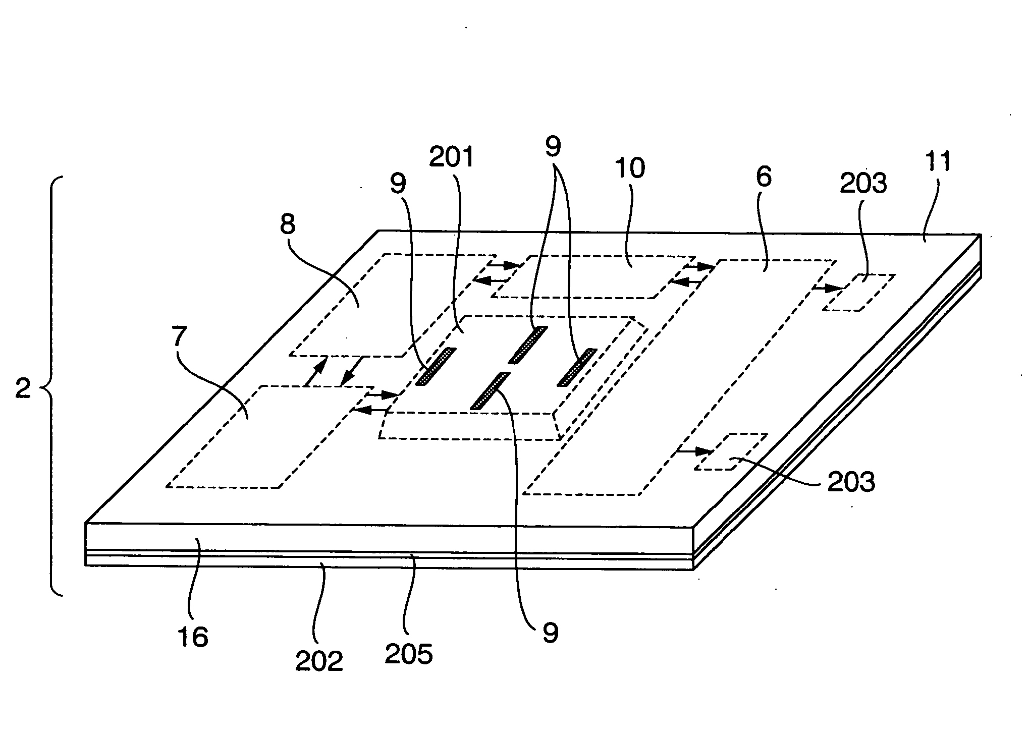
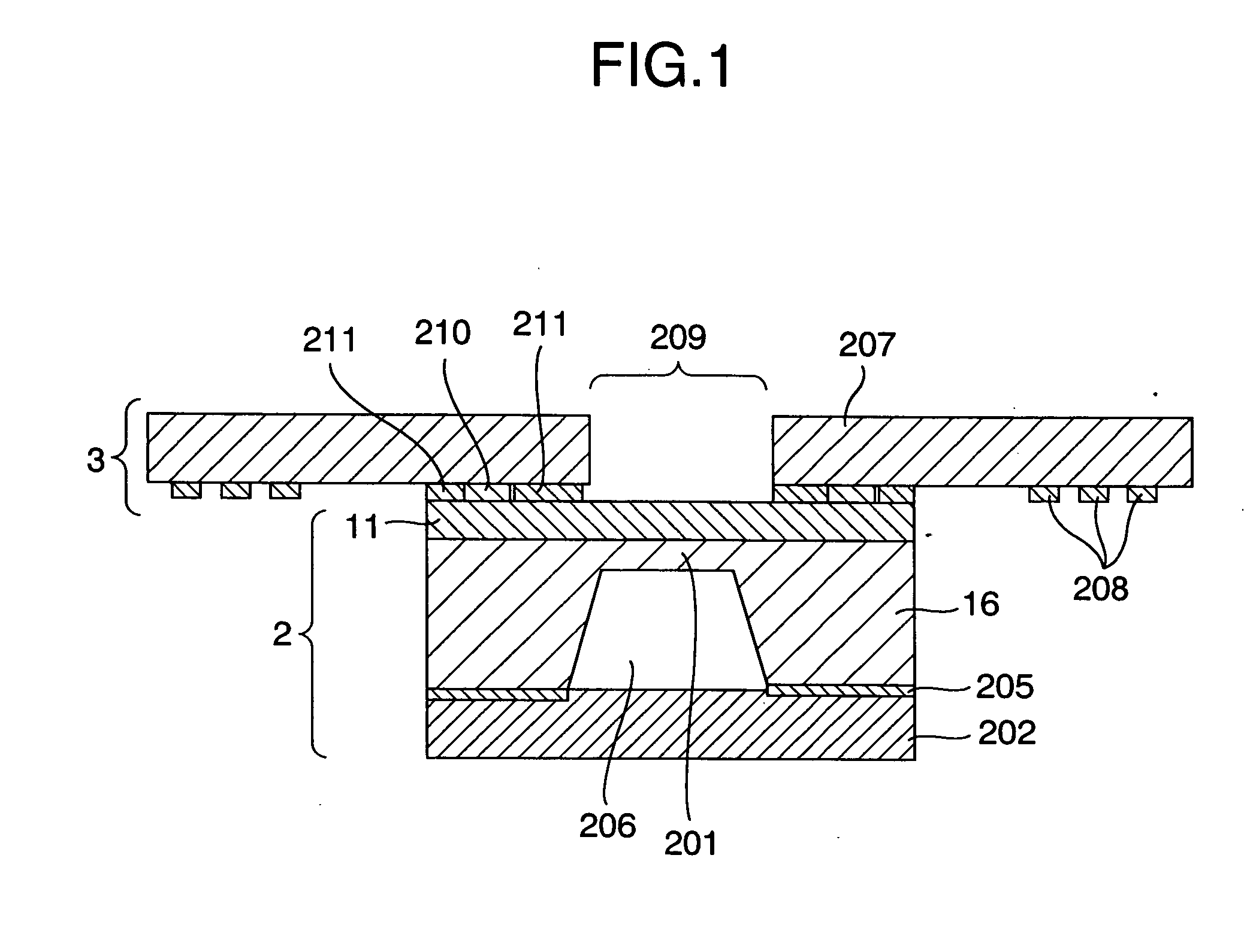
[0082] the present invention is the case where a back surface of the sealing part 202 is brought into contact with the film 207 as shown in FIG. 18. A surface on an opposite side to an element forming surface of the silicon chip is placed on the film 207. The connecting part 210 and the antenna 208 are electrically connected with a metal material 213 such as wire bonding and a metal thin plate. In this case, the diaphragm 201 and the film 207 do not interfere with each other, and therefore, accurate pressure measurement becomes possible. Since rigidity of the film 207 is added to the rigidity of the silicon chip 2, the strain applied to the diaphragm part 201 and the device forming surface 11 can be made small even when an external force such as bending stress is loaded, and therefore, the advantage of being capable of measuring with high accuracy is provided. This embodiment is characterized by including a film or a plate, a silicon chip capable of measuring pressure and an antenna...
first embodiment
[0086]FIG. 22 shows a pressure measuring system using the pressure sensor system 1 of the present invention. The pressure sensor system 1 which measures absolute pressure is provided inside a container 216, and a measurement value of the pressure sensor system 1 is received by the reader 15 provided outside the container 216 by wireless, and is stored in an information storing part in the reader 15 which records information. The film 207 is fixed in the state substantially parallel with an inner wall of the container 216. The surface of the silicon chip on the opposite side to the surface where the diaphragm side is formed is located on the inner wall side of the container 216. In this manner, the inner wall of the container 216 is placed so as to be close to the sealing part 202, and the diaphragm part 201 is placed so as not to interfere with the inner wall of the container 216. As shown in FIG. 23, the surface of the silicon chip 2 where the diaphragm is formed is formed to be lo...
PUM
| Property | Measurement | Unit |
|---|---|---|
| area | aaaaa | aaaaa |
| magnetic permeability | aaaaa | aaaaa |
| pressure | aaaaa | aaaaa |
Abstract
Description
Claims
Application Information


