

Oxide semiconductor electrode, dye-sensitized solar cell, and, method of producing the same
a solar cell and semiconductor technology, applied in the direction of light-sensitive devices, capacitors, electrolytic capacitors, etc., can solve the problems of insufficient adhesive force of conventional adhesives, high production cost of these solar cells, and inability to use general polymer films, etc., to achieve excellent energy conversion efficiency, high productivity, and excellent adhesion stability of respective layers
- Summary
- Abstract
- Description
- Claims
- Application Information
AI Technical Summary
Benefits of technology
Problems solved by technology
Method used
Image

Examples
example 1
1. Formation of Porous Layer
(1) Formation of Oxide Semiconductor Layer-forming Layer
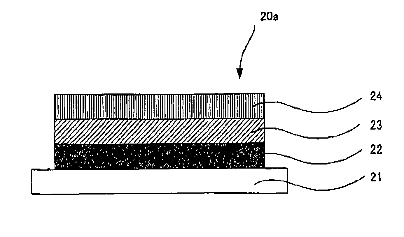
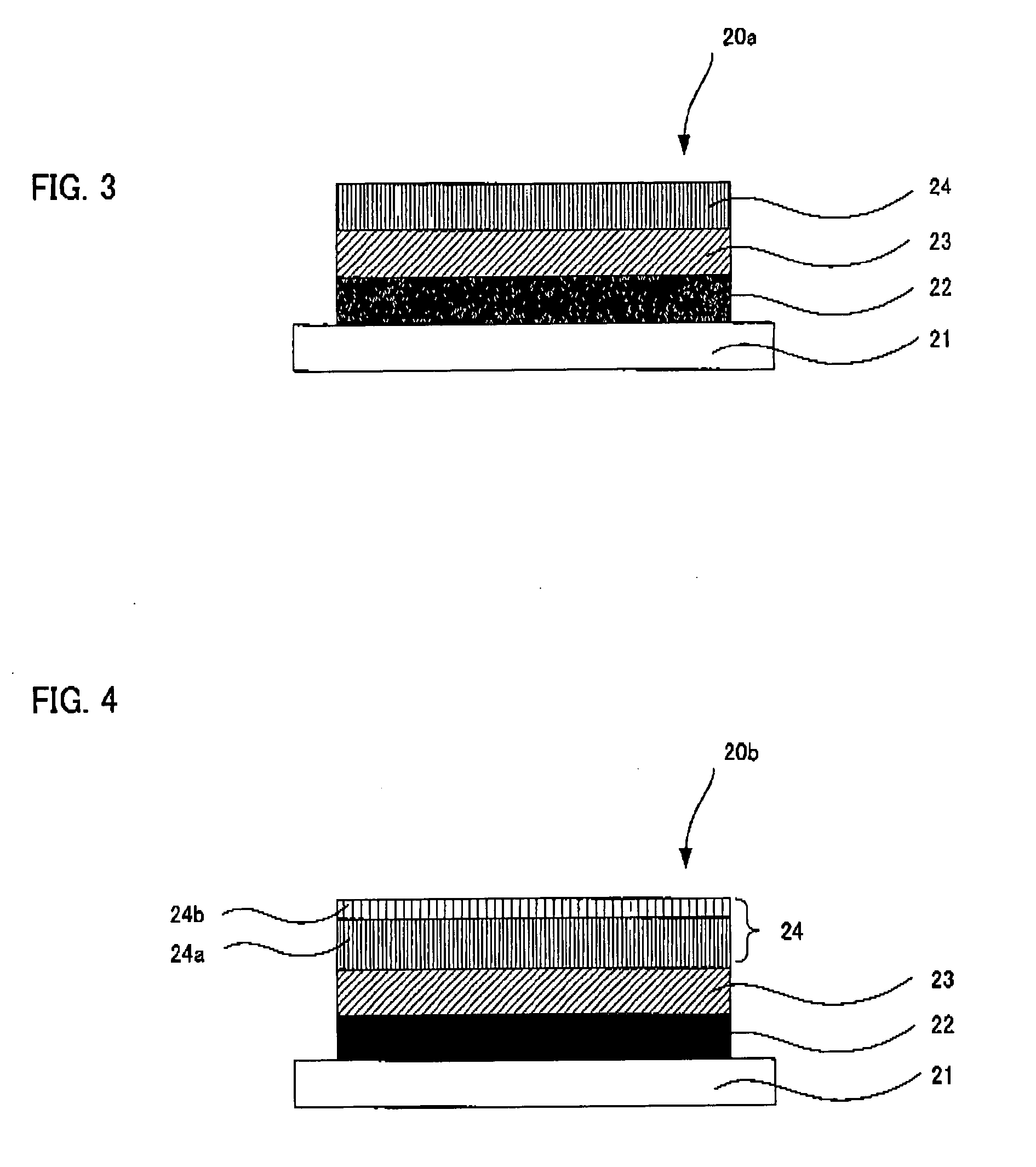
[0406] As an oxide semiconductor layer-forming coating material, a titanium oxide paste having a particle diameter of substantially 13 nm (trade name: Ti-Nanoxide D, manufactured by Solaronix SA) was used. The titanium oxide paste was coated by use of a doctor blade method, followed by leaving at room temperature for 20 minutes, further followed by drying at 100° C. for 30 minutes.
(2) Sintering
[0407] The oxide semiconductor layer-forming layer was sintered at 500° C. for 30 minutes in an electric muffle furnace (tradename: P90, manufactured by DENKEN CO., LTD.) under an atmospheric pressure atmosphere. Thereby, a porous layer formed as a porous body was obtained.
2. Formation of First Electrode Layer
[0408] As a first electrode layer-forming composition, a composition where 0.1 mol / l of indium chloride and 0.005 mol / l of tin chloride were dissolved in ethanol was prepared. Thereafter, the sin...
example 2
[0417] Except that a porous layer was formed by a method below, a dye-sensitized solar cell was prepared by a method similar to that of example 1.
(1) Formation of Intermediate Layer-Forming Layer
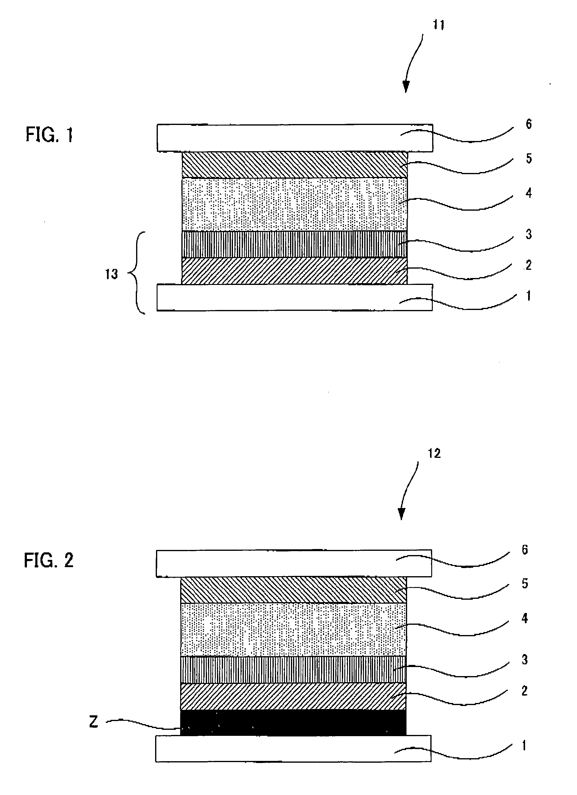
[0418] An intermediate layer-forming coating material was prepared as follows. That is, an acrylic resin (trade name: BR87, manufactured by Mitsubishi Rayon Co., Ltd., molecular weight: 25000 and glass transition temperature: 105° C.) was dissolved in methyl ethyl ketone and toluene, followed by dispersing TiO2 fine particles having a primary particle diameter of 20 nm (trade name: P25, manufactured by NIPPON AEROSIL CO., LTD.) therein by use of a paint shaker so that the TiO2 fine particles and the acrylic resin, respectively, may be 1 mass percent and 10 mass percents, and thereby an intermediate layer-forming coating material was prepared. The intermediate layer-forming coating material was coated by use of a wire bar on an alkali-free glass substrate (thickness: 0.7 mm) prepared as a ...
example 3
[0426] An intermediate layer-forming coating material was prepared as follows. That is, an acrylic resin (trade name: BR87, manufactured by Mitsubishi Rayon Co., Ltd., molecular weight: 25000 and glass transition temperature: 105° C.) mainly made of polymethyl methacrylate was dissolved in methyl ethyl ketone and toluene, followed by dispersing TiO2 fine particles having a primary particle diameter of 20 nm (trade name: P25, manufactured by NIPPON AEROSIL CO., LTD.) therein by use of a homogenizer so that the TiO2 fine particles and the acrylic resin, may be 1 mass percent and 10 mass percents respectively, and thereby an intermediate layer-forming coating material was prepared. The coating material was coated by use of a wire bar on an alkali-free glass substrate (thickness: 0.7 mm) prepared as a heat-resistant substrate and dried. Thereafter, an area of 1 cm×1 cm was masked, an area other than the above was dissolved and removed by use of methyl ethyl ketone and thereby an interme...
PUM
 Abstract
Description
Claims
Application Information